Laser ablation offers precise material removal for microfabrication without the need for masks, making it ideal for rapid prototyping and custom designs, while photolithography excels at producing high-resolution, large-scale patterns with consistent accuracy suited for mass production. Explore the rest of the article to discover which method best fits your project's specific requirements.
Table of Comparison
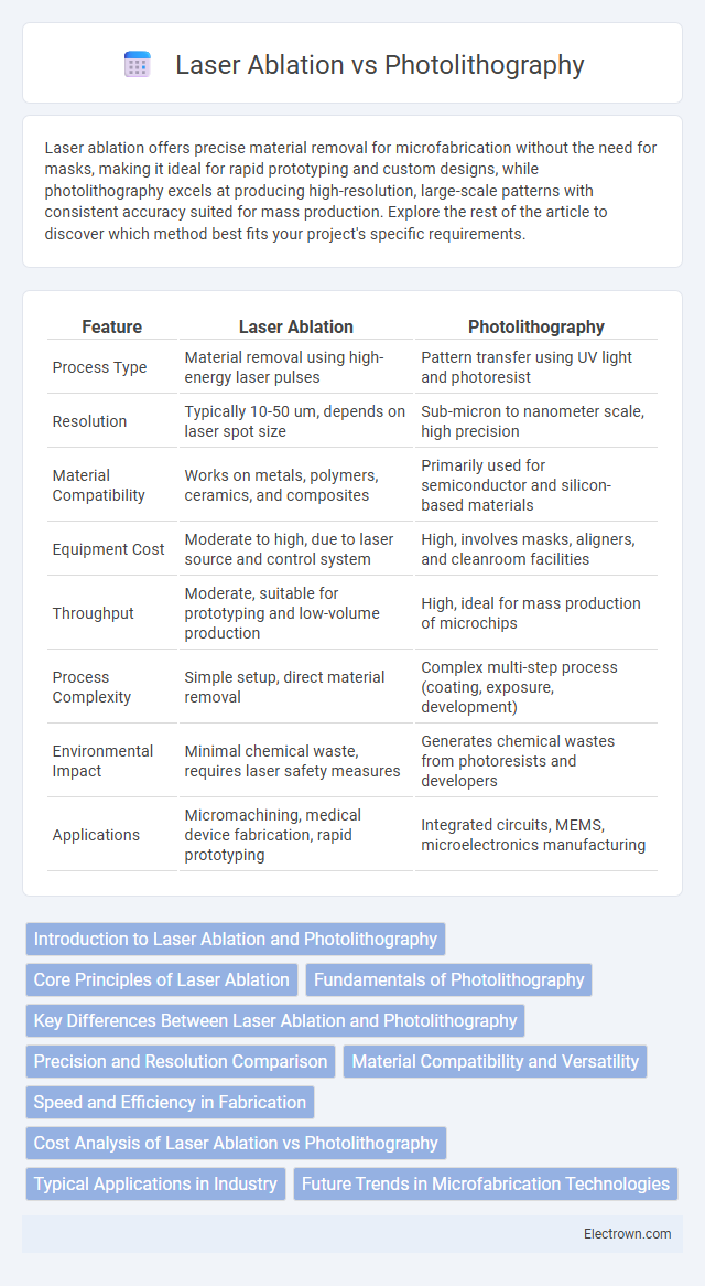
| Feature | Laser Ablation | Photolithography |
|---|---|---|
| Process Type | Material removal using high-energy laser pulses | Pattern transfer using UV light and photoresist |
| Resolution | Typically 10-50 um, depends on laser spot size | Sub-micron to nanometer scale, high precision |
| Material Compatibility | Works on metals, polymers, ceramics, and composites | Primarily used for semiconductor and silicon-based materials |
| Equipment Cost | Moderate to high, due to laser source and control system | High, involves masks, aligners, and cleanroom facilities |
| Throughput | Moderate, suitable for prototyping and low-volume production | High, ideal for mass production of microchips |
| Process Complexity | Simple setup, direct material removal | Complex multi-step process (coating, exposure, development) |
| Environmental Impact | Minimal chemical waste, requires laser safety measures | Generates chemical wastes from photoresists and developers |
| Applications | Micromachining, medical device fabrication, rapid prototyping | Integrated circuits, MEMS, microelectronics manufacturing |
Introduction to Laser Ablation and Photolithography
Laser ablation utilizes high-intensity laser pulses to precisely remove material from a surface, enabling direct patterning with minimal chemical use. Photolithography employs light exposure through a patterned mask to transfer intricate designs onto a photosensitive resist, widely used in semiconductor fabrication. Understanding these processes helps you select the best technique for microfabrication, balancing resolution, speed, and material compatibility.
Core Principles of Laser Ablation
Laser ablation operates by using high-energy laser pulses to precisely remove material from a substrate through rapid vaporization or sublimation, enabling direct patterning without chemical masks. This process relies on controlled energy absorption and thermal confinement to achieve microscale or nanoscale features, making it ideal for complex and flexible designs. Unlike photolithography, laser ablation offers maskless fabrication and can process a wide variety of materials, including metals, polymers, and ceramics.
Fundamentals of Photolithography
Photolithography relies on the use of light to transfer a geometric pattern from a photomask to a light-sensitive chemical photoresist on the substrate, enabling precise microfabrication. This process involves multiple steps, including coating, exposure, development, and etching, to define intricate circuit designs with nanometer-scale resolution. Your choice of photolithography techniques directly impacts the accuracy and scalability of semiconductor manufacturing.
Key Differences Between Laser Ablation and Photolithography
Laser ablation involves direct material removal using high-energy laser pulses, enabling precise patterning on various substrates without masks, while photolithography relies on light exposure through masks to transfer patterns onto photosensitive resists. Laser ablation offers higher flexibility and rapid prototyping for microfabrication, whereas photolithography excels in high-volume, high-resolution semiconductor manufacturing due to its scalability and reproducibility. The choice between these techniques depends on factors such as material type, feature size, throughput requirements, and production cost.
Precision and Resolution Comparison
Laser ablation offers high precision with micrometer-level accuracy, making it ideal for applications requiring fine removal of materials, while photolithography achieves sub-micron resolution through light exposure on photoresist layers, enabling intricate patterning essential for semiconductor fabrication. The resolution of photolithography commonly surpasses that of laser ablation due to its ability to define features below 100 nanometers using advanced techniques like deep ultraviolet (DUV) and extreme ultraviolet (EUV) lithography. Your choice between these methods depends on whether you prioritize direct material removal with flexible patterning (laser ablation) or ultra-high resolution and complex circuit patterning (photolithography).
Material Compatibility and Versatility
Laser ablation offers exceptional material compatibility, enabling precise processing of metals, ceramics, polymers, and composites without the need for masks or chemicals, making it highly versatile for diverse applications. Photolithography excels in producing intricate micro-scale patterns primarily on semiconductor materials like silicon and photoresists but has limited adaptability to non-planar or flexible substrates. Your choice depends on whether you need broad material versatility with laser ablation or high-resolution patterning within semiconductor-compatible materials offered by photolithography.
Speed and Efficiency in Fabrication
Laser ablation offers faster material removal and higher precision without the need for masks, significantly improving fabrication speed and flexibility compared to photolithography. Photolithography, while capable of producing highly detailed microstructures, involves multiple time-consuming steps such as coating, exposure, and development, which reduce overall efficiency. Your choice between these methods depends on the balance between production speed and the complexity of the desired patterns.
Cost Analysis of Laser Ablation vs Photolithography
Laser ablation typically incurs lower initial costs compared to photolithography, as it requires less expensive equipment and fewer cleanroom facilities, making it ideal for small to medium-scale production or prototyping. Photolithography demands significant investment in costly masks, photoresists, and high-precision machinery, driving up fixed costs but benefiting high-volume manufacturing through economies of scale. Your decision should consider project scale and budget constraints to determine whether the cost efficiency of laser ablation or the precision and throughput of photolithography aligns better with your production needs.
Typical Applications in Industry
Laser ablation is widely used in industries such as aerospace and medical device manufacturing for precision material removal and micro-machining, enabling high-resolution patterning on metals, ceramics, and polymers. Photolithography is predominantly employed in semiconductor fabrication, enabling the mass production of integrated circuits, microchips, and microelectromechanical systems (MEMS) with intricate circuit patterns on silicon wafers. Your choice between these technologies depends on the specific application needs, such as material type, feature resolution, and production scale.
Future Trends in Microfabrication Technologies
Future trends in microfabrication technologies reveal increasing adoption of laser ablation due to its precision, speed, and ability to process diverse materials without masks, contrasting with photolithography's reliance on complex chemical processes and photomasks. Innovations in ultrafast lasers and AI-driven control systems are enhancing laser ablation's scalability for high-volume manufacturing, positioning it as a flexible alternative to traditional photolithography in semiconductor and biomedical device fabrication. Understanding these advancements can help you select the most efficient microfabrication method to meet the evolving demands of precision engineering and miniaturization.
Laser ablation vs Photolithography Infographic