Bulk CMOS technology, known for its cost-effectiveness and mature fabrication process, encounters challenges in scaling with increased leakage current and parasitic capacitance, whereas SOI CMOS offers superior performance with reduced power consumption and enhanced speed due to its insulating silicon-on-insulator substrate. Explore the following article to understand how these differences impact your semiconductor device choices and overall design efficiency.
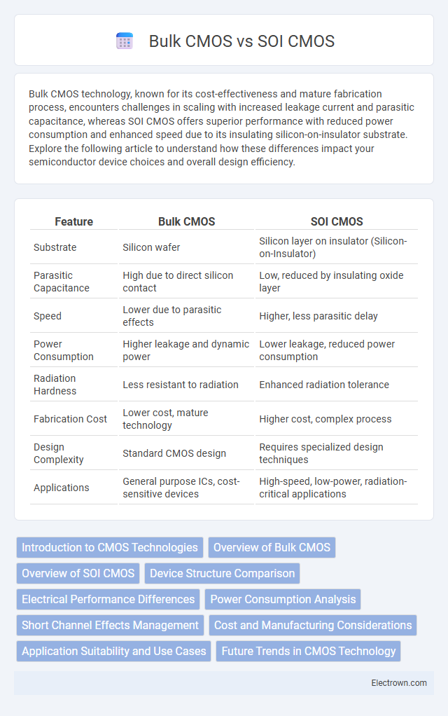
Table of Comparison
| Feature | Bulk CMOS | SOI CMOS |
|---|---|---|
| Substrate | Silicon wafer | Silicon layer on insulator (Silicon-on-Insulator) |
| Parasitic Capacitance | High due to direct silicon contact | Low, reduced by insulating oxide layer |
| Speed | Lower due to parasitic effects | Higher, less parasitic delay |
| Power Consumption | Higher leakage and dynamic power | Lower leakage, reduced power consumption |
| Radiation Hardness | Less resistant to radiation | Enhanced radiation tolerance |
| Fabrication Cost | Lower cost, mature technology | Higher cost, complex process |
| Design Complexity | Standard CMOS design | Requires specialized design techniques |
| Applications | General purpose ICs, cost-sensitive devices | High-speed, low-power, radiation-critical applications |
Introduction to CMOS Technologies
Bulk CMOS technology uses a silicon substrate where transistors are directly formed, offering cost-effective manufacturing and mature process integration. SOI CMOS incorporates a thin layer of silicon on top of an insulating oxide layer, reducing parasitic capacitance and improving power efficiency, speed, and radiation hardness. Your choice between Bulk and SOI CMOS impacts device performance, power consumption, and overall system reliability in semiconductor applications.
Overview of Bulk CMOS
Bulk CMOS technology utilizes a silicon substrate where transistors are formed directly in the bulk material, offering cost-effective manufacturing and well-established fabrication processes. This approach typically results in higher parasitic capacitances and leakage currents compared to SOI CMOS, impacting power efficiency and switching speed. Your choice of Bulk CMOS is suitable for applications prioritizing low cost and mature technology over ultra-low power consumption and high-speed performance.
Overview of SOI CMOS
SOI CMOS (Silicon-On-Insulator Complementary Metal-Oxide-Semiconductor) technology integrates a thin silicon layer separated from the bulk substrate by an insulating oxide layer, significantly reducing parasitic capacitance and improving transistor switching speeds. This structure enhances device performance, reduces power consumption, and mitigates short-channel effects compared to traditional Bulk CMOS, making SOI CMOS ideal for high-speed and low-power applications. Your circuits benefit from improved noise immunity and scalability in advanced semiconductor processes using SOI CMOS technology.
Device Structure Comparison
Bulk CMOS features a silicon substrate where devices are built directly on the bulk silicon, resulting in a straightforward structure with a well-established fabrication process. SOI CMOS utilizes a thin silicon layer separated from the bulk substrate by a buried oxide (BOX) layer, minimizing parasitic capacitance and improving device isolation. The BOX layer in SOI significantly reduces leakage current and short-channel effects, enhancing performance in high-speed and low-power applications.
Electrical Performance Differences
Bulk CMOS devices exhibit higher parasitic capacitance and leakage currents due to the silicon substrate, which can degrade electrical performance at high frequencies. SOI CMOS technology reduces parasitic capacitances and leakage by isolating the transistor channels with a thin buried oxide layer, leading to improved switching speeds and lower power consumption. This results in SOI CMOS achieving better performance in high-speed and low-power applications compared to bulk CMOS.
Power Consumption Analysis
Bulk CMOS technology exhibits higher power consumption primarily due to increased parasitic capacitances and leakage currents from the substrate. SOI CMOS reduces power consumption by isolating the active device region with a buried oxide layer, thereby minimizing leakage currents and junction capacitances. This isolation enables lower threshold voltages and improved short-channel effects, leading to significant dynamic and static power savings in low-power applications.
Short Channel Effects Management
SOI CMOS technology significantly improves short channel effects management by reducing parasitic capacitance and suppressing leakage currents through the buried oxide layer, which enhances device scalability at nanometer nodes. Bulk CMOS faces greater challenges with short channel effects due to the direct silicon substrate, resulting in higher drain-induced barrier lowering (DIBL) and threshold voltage roll-off. Your choice of SOI CMOS can optimize performance and power efficiency in advanced integrated circuits by enhancing electrostatic control in short-channel devices.
Cost and Manufacturing Considerations
Bulk CMOS technology offers lower manufacturing costs due to established fabrication processes and widespread availability of silicon wafers, making it ideal for high-volume production. SOI CMOS involves more complex and costly fabrication steps, including the production of SOI wafers with buried oxide layers, which increases overall expenses but improves device performance and reduces parasitic capacitance. Cost considerations favor Bulk CMOS for budget-sensitive projects, while SOI CMOS is preferred when advanced performance and power efficiency justify higher manufacturing investments.
Application Suitability and Use Cases
Bulk CMOS technology is widely used in cost-sensitive applications such as microcontrollers, digital logic circuits, and power management ICs due to its mature fabrication process and lower manufacturing costs. SOI CMOS excels in high-performance and low-power applications including RF radios, high-speed processors, and radiation-hardened devices, offering improved speed, reduced parasitic capacitance, and enhanced resistance to soft errors. Your choice between Bulk CMOS and SOI CMOS should consider performance requirements, power efficiency, and environmental conditions of the target application.
Future Trends in CMOS Technology
Future trends in CMOS technology emphasize the shift from Bulk CMOS to SOI CMOS due to SOI's superior performance in reducing parasitic capacitance, enhancing speed, and lowering power consumption. SOI CMOS is increasingly favored in advanced nodes for applications requiring high-speed computing and low leakage currents, aligning with industry demands for energy-efficient devices. Your design choices will benefit from considering SOI CMOS as it supports scaling challenges and improved device reliability in next-generation semiconductor technologies.
Bulk CMOS vs SOI CMOS Infographic