Split gate transistors offer improved control over channel formation and reduced short-channel effects compared to single gate transistors, enhancing device performance and reliability. Explore the rest of the article to understand how these differences impact your semiconductor applications.
Table of Comparison
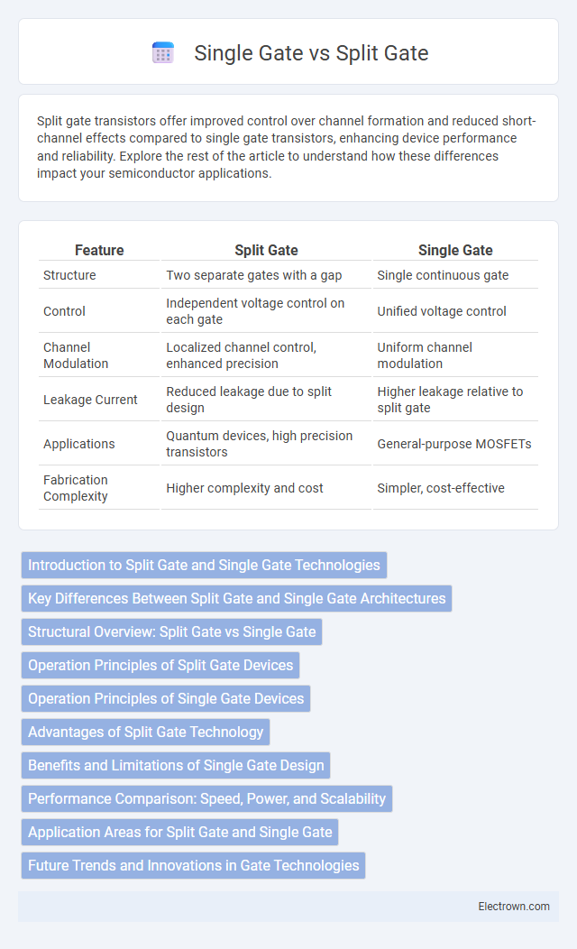
| Feature | Split Gate | Single Gate |
|---|---|---|
| Structure | Two separate gates with a gap | Single continuous gate |
| Control | Independent voltage control on each gate | Unified voltage control |
| Channel Modulation | Localized channel control, enhanced precision | Uniform channel modulation |
| Leakage Current | Reduced leakage due to split design | Higher leakage relative to split gate |
| Applications | Quantum devices, high precision transistors | General-purpose MOSFETs |
| Fabrication Complexity | Higher complexity and cost | Simpler, cost-effective |
Introduction to Split Gate and Single Gate Technologies
Split gate and single gate technologies represent two distinct approaches in transistor design, crucial for controlling electrical current in semiconductor devices. Single gate transistors use one gate electrode to modulate the channel, providing simpler fabrication but limited electrostatic control. Split gate transistors employ two separate gate electrodes, enhancing electrostatic control and reducing short-channel effects, thereby improving device performance in advanced integrated circuits.
Key Differences Between Split Gate and Single Gate Architectures
Split gate architecture features two independently controlled gates that improve electrostatic control and reduce short channel effects, enhancing device performance in advanced CMOS technologies. Single gate architecture, with only one gate controlling the channel, typically faces greater leakage currents and less precise channel modulation as device dimensions scale down. The split gate design offers superior scalability, better threshold voltage control, and improved suppression of drain-induced barrier lowering compared to single gate devices.
Structural Overview: Split Gate vs Single Gate
The split gate transistor design incorporates two separate gate electrodes controlling distinct regions of the channel, enhancing electrostatic control and reducing short-channel effects compared to the single gate structure, which uses a single continuous gate electrode over the channel. Split gate layouts enable better suppression of leakage current by locally modulating the electric field, while single gate devices often experience increased drain-induced barrier lowering (DIBL) due to less precise control. Semiconductor manufacturers prefer split gate architectures in scaling down transistors to nanometer dimensions for improved performance and power efficiency over traditional single gate configurations.
Operation Principles of Split Gate Devices
Split gate devices operate by independently controlling separate gate electrodes to modulate the channel conductivity with enhanced precision, unlike single gate devices that use a single electrode for this purpose. This independent control allows for better electrostatic control over the channel, reducing short-channel effects and enabling improved threshold voltage tuning. Your device performance benefits from increased scalability and reduced leakage currents due to the distinct operation principles of split gate structures.
Operation Principles of Single Gate Devices
Single gate devices operate by controlling the current flow through a semiconductor channel using a single gate electrode to modulate the channel conductivity via an electric field. This gate voltage creates an electric field that influences the charge carriers in the channel, enabling the device to switch between on and off states. Your device's performance depends on how efficiently this single gate can control the channel, impacting parameters like threshold voltage, subthreshold slope, and overall switching speed.
Advantages of Split Gate Technology
Split gate technology offers enhanced control over the transistor channel, enabling reduced short-channel effects and improved device scaling for advanced semiconductor nodes. It provides better electrostatic integrity, which minimizes leakage currents and boosts overall power efficiency compared to single gate designs. Your circuits benefit from higher drive current and improved threshold voltage control, resulting in faster switching speeds and greater reliability in nanoscale devices.
Benefits and Limitations of Single Gate Design
Single gate transistor design offers simplicity and easier fabrication, making it cost-effective for many semiconductor applications. However, single gate devices face limitations like increased short-channel effects and reduced control over the channel, which hampers performance at smaller technology nodes. Your choice depends on whether prioritizing manufacturing ease outweighs the need for enhanced electrostatic control found in split gate structures.
Performance Comparison: Speed, Power, and Scalability
Split gate transistors enhance speed by reducing parasitic capacitance compared to single gate devices, resulting in faster switching times. They offer superior power efficiency due to lower leakage currents and improved control over short-channel effects, making them ideal for low-power applications. Scalability favors split gate designs as they maintain performance advantages at smaller technology nodes, addressing challenges faced by single gate transistors in advanced semiconductor processes.
Application Areas for Split Gate and Single Gate
Split gate transistors excel in applications requiring precise threshold voltage control and reduced short-channel effects, making them ideal for advanced memory devices like DRAM and flash memory. Single gate transistors, favored for their simpler design, are widely used in general-purpose digital logic circuits and analog applications where standard performance suffices. Your choice between split gate and single gate depends on the specific requirements for device scaling, power efficiency, and noise immunity in your application area.
Future Trends and Innovations in Gate Technologies
Split gate technology offers advanced control over channel conduction, enabling lower power consumption and enhanced scalability compared to traditional single gate designs, which are reaching physical scaling limits. Future trends indicate a shift toward multi-gate architectures like split gates and gate-all-around (GAA) transistors to sustain Moore's Law by improving electrostatic control and minimizing short-channel effects. Your adoption of split gate transistors can drive innovation in high-performance, energy-efficient semiconductors crucial for next-generation AI, 5G, and quantum computing applications.
Split gate vs single gate Infographic