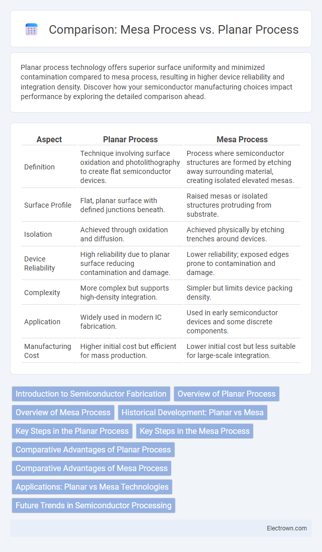
Planar process technology offers superior surface uniformity and minimized contamination compared to mesa process, resulting in higher device reliability and integration density. Discover how your semiconductor manufacturing choices impact performance by exploring the detailed comparison ahead.
Table of Comparison
| Aspect | Planar Process | Mesa Process |
|---|---|---|
| Definition | Technique involving surface oxidation and photolithography to create flat semiconductor devices. | Process where semiconductor structures are formed by etching away surrounding material, creating isolated elevated mesas. |
| Surface Profile | Flat, planar surface with defined junctions beneath. | Raised mesas or isolated structures protruding from substrate. |
| Isolation | Achieved through oxidation and diffusion. | Achieved physically by etching trenches around devices. |
| Device Reliability | High reliability due to planar surface reducing contamination and damage. | Lower reliability; exposed edges prone to contamination and damage. |
| Complexity | More complex but supports high-density integration. | Simpler but limits device packing density. |
| Application | Widely used in modern IC fabrication. | Used in early semiconductor devices and some discrete components. |
| Manufacturing Cost | Higher initial cost but efficient for mass production. | Lower initial cost but less suitable for large-scale integration. |
Introduction to Semiconductor Fabrication
The planar process in semiconductor fabrication employs oxide layers to create flat, stable surfaces essential for reliable integrated circuits, enhancing device performance and scalability. Mesa processing involves etching semiconductor materials into raised areas, which can cause surface defects and reliability issues but allows for simpler isolation of devices. Understanding these methods helps you choose the appropriate technique based on the desired device complexity and manufacturing requirements.
Overview of Planar Process
The planar process is a semiconductor fabrication technique that enables the creation of integrated circuits on a flat silicon wafer surface using oxidation, photolithography, and diffusion steps. This method improves device reliability and allows for high-density circuit integration by forming transistors within a thin oxide layer, unlike the mesa process, which etches away material to isolate devices. Your microelectronics designs benefit from the planar process's precision and scalability, making it the foundation for modern chip manufacturing.
Overview of Mesa Process
The Mesa process is a semiconductor fabrication technique that involves etching trenches around device areas to isolate components by physically elevating active regions above the substrate surface. This method creates mesa structures that improve electrical isolation but can lead to increased surface recombination and reliability issues compared to planar processes. Mesa technology is primarily used in compound semiconductor devices such as gallium arsenide (GaAs) due to its straightforward implementation for high-frequency applications.
Historical Development: Planar vs Mesa
The planar process, developed by Jean Hoerni in the late 1950s, revolutionized semiconductor manufacturing by enabling flat transistor surfaces on silicon wafers, advancing integrated circuit complexity and reliability. In contrast, the earlier mesa process, characterized by etching raised transistor structures, faced limitations in device isolation and contamination, which hindered scaling and mass production. Your understanding of modern semiconductor fabrication benefits from recognizing how the planar process's innovations paved the way for current microelectronics, surpassing the mesa approach in precision and efficiency.
Key Steps in the Planar Process
The planar process involves key steps such as oxidation to form a protective silicon dioxide layer, photolithography for pattern definition, and selective etching to create precise semiconductor structures. Dopant diffusion or ion implantation follows to modify electrical properties, while additional oxide layers provide insulation and surface passivation. Your semiconductor device benefits from these carefully controlled steps to achieve improved performance and reliability compared to mesa-structured devices.
Key Steps in the Mesa Process
The Mesa process involves etching away specific areas of the semiconductor wafer to form isolated mesa structures, which serve as the active regions of devices. Key steps include photolithography to define the mesa pattern, followed by anisotropic or isotropic etching techniques to remove unwanted material and create well-defined vertical sidewalls. Your device's performance often depends on precise control of these etching steps, which influence the mesa's dimensions and electrical isolation.
Comparative Advantages of Planar Process
The planar process offers superior scalability and integration capabilities compared to the mesa process, enabling higher transistor density and improved consistency in semiconductor fabrication. Enhanced planarization reduces surface irregularities, facilitating more reliable photolithography and precise layer stacking essential for modern integrated circuits. Its widespread adoption in CMOS technology underscores the planar process's efficiency in producing complex, high-performance microchips with lower defect rates and better electrical characteristics.
Comparative Advantages of Mesa Process
Mesa process offers superior isolation and reduced parasitic capacitance compared to the planar process, enhancing device performance in high-frequency applications. It enables precise control over device geometry by etching away unwanted areas, resulting in better-defined device structures and improved reliability. Your choice of the mesa process can lead to enhanced thermal management and reduced leakage currents in semiconductor devices.
Applications: Planar vs Mesa Technologies
Planar process technology excels in integrated circuits, memory chips, and microprocessors due to its precise control over transistor structures, offering higher device density and reliability. Mesa process technology is often applied in photonics and power devices where isolation and ruggedness are critical, such as in LED fabrication and high-voltage components. Understanding your application requirements helps determine whether the planar process's scalability or mesa process's robustness aligns better with your technology needs.
Future Trends in Semiconductor Processing
Future trends in semiconductor processing emphasize the integration of planar process improvements with advanced mesa process techniques to enhance device performance and scalability. Innovations such as atomic layer deposition and selective area growth optimize planar surfaces, while mesa processing evolves with precision etching and novel passivation methods for high-power and high-frequency applications. The convergence of these processes supports the development of smaller, more efficient semiconductor devices with improved electrical characteristics and thermal management.
Planar process vs mesa process Infographic