Wafer-level packaging offers a compact, high-performance solution by assembling the entire wafer before dicing, resulting in reduced size and enhanced electrical performance compared to die-level packaging, which processes individual dies separately and allows more flexibility in customization. Exploring the differences between these packaging methods can help you choose the best option for your semiconductor device needs--read on to learn more.
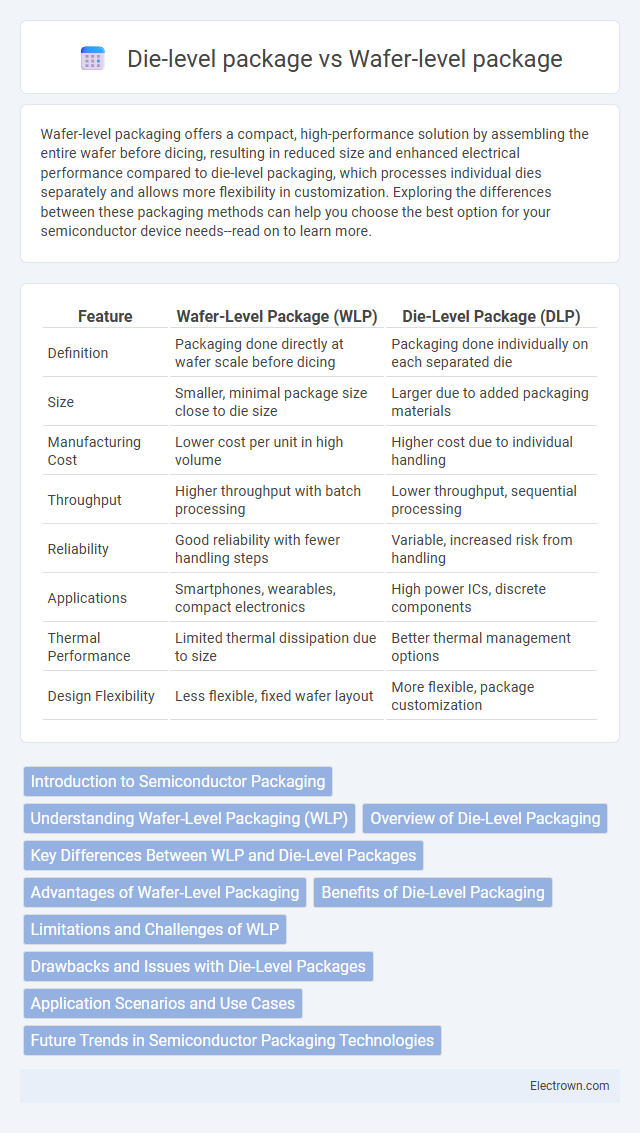
Table of Comparison
| Feature | Wafer-Level Package (WLP) | Die-Level Package (DLP) |
|---|---|---|
| Definition | Packaging done directly at wafer scale before dicing | Packaging done individually on each separated die |
| Size | Smaller, minimal package size close to die size | Larger due to added packaging materials |
| Manufacturing Cost | Lower cost per unit in high volume | Higher cost due to individual handling |
| Throughput | Higher throughput with batch processing | Lower throughput, sequential processing |
| Reliability | Good reliability with fewer handling steps | Variable, increased risk from handling |
| Applications | Smartphones, wearables, compact electronics | High power ICs, discrete components |
| Thermal Performance | Limited thermal dissipation due to size | Better thermal management options |
| Design Flexibility | Less flexible, fixed wafer layout | More flexible, package customization |
Introduction to Semiconductor Packaging
Wafer-level packaging (WLP) integrates packaging processes directly on the semiconductor wafer before it is diced into individual chips, offering improved electrical performance and reduced package size compared to die-level packaging, which involves encapsulating each die independently after separation. WLP enhances heat dissipation and signal integrity by minimizing interconnect lengths and allows for higher production throughput and lower manufacturing costs in advanced semiconductor devices. Your choice between these packaging methods impacts device reliability, form factor, and overall system performance in applications ranging from mobile electronics to high-performance computing.
Understanding Wafer-Level Packaging (WLP)
Wafer-Level Packaging (WLP) involves packaging integrated circuits directly at the wafer scale before dicing, enabling smaller package sizes, improved electrical performance, and reduced manufacturing costs compared to Die-Level Packaging (DLP). WLP offers advantages in miniaturization and high-density interconnects, making it ideal for applications requiring compact, high-performance semiconductor devices. Your choice between WLP and DLP should consider factors like device complexity, thermal management, and overall production efficiency.
Overview of Die-Level Packaging
Die-level packaging involves encapsulating individual semiconductor dies separately, offering enhanced customization and improved thermal management compared to wafer-level packaging. This method supports complex interconnect structures and facilitates efficient testing and replacement of defective dies, reducing overall production costs. Die-level packages typically provide superior electrical performance and reliability, making them ideal for high-performance applications such as CPUs and memory modules.
Key Differences Between WLP and Die-Level Packages
Wafer-level packages (WLP) are fabricated directly on the entire wafer, offering superior miniaturization and improved electrical performance due to reduced interconnect lengths, while die-level packages (DLP) involve packaging individual chips after wafer dicing, allowing flexibility in package types. WLP enhances thermal management and cost efficiency in high-volume production, whereas DLP provides easier defect isolation and testing at the die stage. Your choice between WLP and DLP depends on factors like device complexity, production volume, and cost constraints.
Advantages of Wafer-Level Packaging
Wafer-level packaging (WLP) offers significant advantages including reduced package size and weight by integrating the packaging process directly at the wafer stage, leading to improved electrical performance due to shorter interconnect lengths. Enhanced thermal management and higher throughput in manufacturing processes result in lower production costs compared to die-level packaging. WLP also enables better scalability for advanced semiconductor nodes, supporting the demands of miniaturized and high-performance electronic devices.
Benefits of Die-Level Packaging
Die-level packaging offers significant benefits, including enhanced thermal management and improved electrical performance due to shorter interconnects directly on each individual die. This packaging method enables higher yield and lower costs by isolating defects to single die rather than entire wafers, leading to better overall reliability. Die-level packaging also provides greater flexibility in customizing packages for diverse applications and supports advanced chip functionalities with optimized signal integrity.
Limitations and Challenges of WLP
Wafer-level packaging (WLP) faces limitations such as size constraints due to the thin wafer and limited space for redistribution layers, impacting complex circuit designs. Thermal management and mechanical stress are significant challenges, as the thin wafer structure can lead to warping and reliability issues under operational conditions. Your design may also encounter difficulties with fine-pitch interconnections and yield losses during wafer thinning and dicing processes compared to die-level packaging.
Drawbacks and Issues with Die-Level Packages
Die-level packages often face challenges such as limited thermal dissipation and increased risk of mechanical stress due to the lack of a robust protective encapsulation compared to wafer-level packages. They tend to have higher production costs and longer assembly times because each die must be packaged individually, which increases the potential for handling damage and contamination. The variability in die-level packaging processes can lead to inconsistent electrical performance and lower yield rates compared to the more standardized and integrated wafer-level packaging methods.
Application Scenarios and Use Cases
Wafer-level packages (WLP) are ideal for compact, high-volume applications such as mobile devices and consumer electronics where miniaturization and cost efficiency are critical. Die-level packages (DLP) excel in scenarios demanding enhanced thermal management and mechanical robustness, like automotive electronics and industrial sensors. Choosing between WLP and DLP depends on your product's size constraints, performance requirements, and environmental conditions.
Future Trends in Semiconductor Packaging Technologies
Wafer-level packaging (WLP) shows strong potential for future semiconductor packaging technologies due to its ability to enable higher integration density and improved electrical performance compared to die-level packaging. Advanced WLP techniques like fan-out wafer-level packaging (FOWLP) are driving trends toward smaller form factors and enhanced thermal management, critical for next-generation high-speed devices. Your choice between WLP and die-level packaging will impact device miniaturization, manufacturing efficiency, and overall system reliability in emerging applications like 5G, AI, and IoT.
Wafer-level package vs Die-level package Infographic