NPNL and PNPN structures differ primarily in their transistor arrangements and switching behavior, with NPNL using a combination of NPN and PNP transistors for faster switching speed and improved efficiency in power electronics. Explore the rest of the article to understand how these structures impact your circuit design and performance.
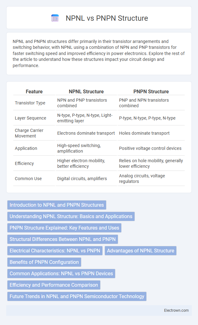
Table of Comparison
| Feature | NPNL Structure | PNPN Structure |
|---|---|---|
| Transistor Type | NPN and PNP transistors combined | PNP and NPN transistors combined |
| Layer Sequence | N-type, P-type, N-type, Light-emitting layer | P-type, N-type, P-type, N-type |
| Charge Carrier Movement | Electrons dominate transport | Holes dominate transport |
| Application | High-speed switching, amplification | Positive voltage control devices |
| Efficiency | Higher electron mobility, better efficiency | Relies on hole mobility, generally lower efficiency |
| Common Use | Digital circuits, amplifiers | Analog circuits, voltage regulators |
Introduction to NPNL and PNPN Structures
NPNL and PNPN structures are semiconductor configurations primarily used in electronic devices such as transistors and thyristors. An NPNL structure typically consists of alternating layers of N-type and P-type materials with an additional layer to enhance performance, whereas a PNPN structure features four alternating layers (PNPN) forming a thyristor with distinct switching characteristics. Understanding these structures is crucial for optimizing your circuit design and achieving desired electrical control functionalities.
Understanding NPNL Structure: Basics and Applications
The NPNL structure, characterized by alternating n-type and p-type semiconductor layers arranged as n-p-n-layers, enhances charge carrier mobility and switching speed in devices such as transistors and diodes. This configuration improves current amplification and voltage regulation, making it essential for applications in high-frequency amplifiers and power control circuits. Understanding the electrical properties and layer doping concentrations of NPNL components is crucial for optimizing performance in semiconductor frameworks.
PNPN Structure Explained: Key Features and Uses
The PNPN structure, also known as a thyristor, consists of four alternating layers of p-type and n-type semiconductor material, creating three junctions that enable it to act as a switch in electronic circuits. Key features include its ability to maintain a conducting state after being triggered by a gate signal, making it ideal for controlling high-voltage and high-current loads. Your use of a PNPN device is common in applications such as motor control, light dimming, and overvoltage protection due to its efficient switching and latching capabilities.
Structural Differences Between NPNL and PNPN
The NPNL (Negative-Positive-Negative-Linear) structure comprises a sequence where two negative layers flank a positive layer directly followed by a linear segment, while the PNPN (Positive-Negative-Positive-Negative) structure alternates positive and negative layers in a four-layer stack. Your choice between NPNL and PNPN configurations impacts electrical characteristics like charge distribution and switching speed, as the PNPN structure often facilitates thyristor action in semiconductor devices. Structural differences influence device performance in applications such as rectifiers and transistors, making layer arrangement critical for optimizing semiconductor behavior.
Electrical Characteristics: NPNL vs PNPN
NPNL (NPN Layer) and PNPN (thyristor) structures exhibit distinct electrical characteristics crucial for switching applications; NPNL devices typically show faster switching speeds with lower on-state voltage drop, making them ideal for high-frequency operations. PNPN devices, characterized by four alternating layers (P-N-P-N), provide latching behavior and high holding current, enabling stable bistable conduction once triggered, commonly used in latch and trigger circuits. Analyzing breakdown voltages, NPNL devices generally offer higher reverse voltage tolerance, while PNPN structures excel in controlled turn-off features due to their layered regenerative feedback mechanism.
Advantages of NPNL Structure
The NPNL structure offers superior thermal stability and higher voltage handling compared to the PNPN configuration, making it ideal for high-power applications. Its simpler design reduces manufacturing complexity and improves switching speed, enhancing overall efficiency. You benefit from the NPNL structure's improved electrical performance and reliability in demanding environments.
Benefits of PNPN Configuration
PNPN configurations offer enhanced switching speed and greater current handling capacity compared to NPNL structures, making them ideal for high-power applications. Their layered semiconductor design reduces power loss and improves efficiency, ensuring reliable performance under demanding conditions. Your electronic circuits benefit from increased stability and improved thermal management with the PNPN structure.
Common Applications: NPNL vs PNPN Devices
NPNL structures are predominantly used in low-power switching and amplification applications due to their simpler design and faster switching speeds. PNPN devices, known as thyristors or silicon-controlled rectifiers (SCRs), are essential in high-power applications such as AC power control, motor drives, and voltage regulation, where controlled switching of large currents is crucial. Your choice between NPNL and PNPN devices depends on the power handling requirements and switching characteristics needed in your electronic circuit.
Efficiency and Performance Comparison
NPNL structures exhibit higher efficiency in high-speed switching applications due to their lower charge storage and faster carrier recombination compared to PNPN devices. Your choice of an NPNL structure can enhance performance by reducing turn-off time, which is critical in power electronics and RF circuits. In contrast, PNPN structures, often found in thyristors, provide better latching capability but typically suffer from slower response and increased power loss under dynamic conditions.
Future Trends in NPNL and PNPN Semiconductor Technology
Future trends in NPNL and PNPN semiconductor technology emphasize enhanced switching speeds, reduced power consumption, and improved thermal stability for high-frequency and high-power applications. Advances in material science, such as wide bandgap semiconductors like GaN and SiC, are driving the evolution of both NPNL and PNPN structures, enabling devices to operate efficiently at higher voltages and temperatures. Your choice between NPNL and PNPN components will increasingly depend on specific application requirements related to speed, power handling, and integration with emerging semiconductor materials.
NPNL vs PNPN structure Infographic