Junction capacitance arises from the depletion region at a PN junction, varying with the applied voltage and impacting high-frequency device performance, while diffusion capacitance results from the charge storage due to carrier injection and is significant under forward bias conditions. Understanding the differences between these capacitances can help you optimize semiconductor device design and operation; continue reading to explore their roles in electronic applications.
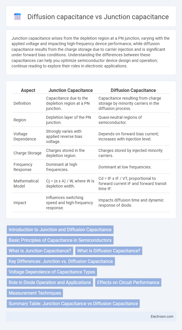
Table of Comparison
| Aspect | Junction Capacitance | Diffusion Capacitance |
|---|---|---|
| Definition | Capacitance due to the depletion region at a PN junction. | Capacitance resulting from charge storage by minority carriers in the diffusion process. |
| Region | Depletion layer of the PN junction. | Quasi-neutral regions of semiconductor. |
| Voltage Dependence | Strongly varies with applied reverse bias voltage. | Depends on forward bias current; increases with injection level. |
| Charge Storage | Charges stored in the depletion region. | Charges stored by injected minority carriers. |
| Frequency Response | Dominant at high frequencies. | Dominant at low frequencies. |
| Mathematical Model | Cj = (e x A) / W, where W is depletion width. | Cd = tF x IF / VT, proportional to forward current IF and forward transit time tF. |
| Impact | Influences switching speed and high-frequency response. | Impacts diffusion time and dynamic response of diode. |
Introduction to Junction and Diffusion Capacitance
Junction capacitance arises from the depletion region in a diode or transistor, where charge separation at the p-n junction behaves like a dielectric in a capacitor, influencing the device's frequency response. Diffusion capacitance occurs due to the storage of minority carriers injected across the junction, significantly impacting the transient response in forward-biased conditions. Understanding these capacitances is crucial for optimizing semiconductor device performance in high-speed and analog circuit applications.
Basic Principles of Capacitance in Semiconductors
Junction capacitance in semiconductors arises from the depletion region acting as a dielectric between p-n junctions, varying inversely with the depletion width and directly affecting device switching speed. Diffusion capacitance, significant in forward-biased conditions, results from charge storage due to minority carrier injection in the quasi-neutral regions, influencing transient response and frequency behavior. Understanding the interplay between these capacitances is crucial for designing high-performance semiconductor devices like diodes and transistors.
What is Junction Capacitance?
Junction capacitance, also known as depletion capacitance, occurs at the p-n junction of a semiconductor diode and is due to the charge stored in the depletion region when the junction is reverse-biased. This capacitance varies with the applied voltage because the width of the depletion region changes, directly affecting the charge storage capability. It plays a crucial role in high-frequency circuit applications by influencing the diode's switching speed and reactive impedance.
What is Diffusion Capacitance?
Diffusion capacitance arises in a forward-biased PN junction due to the storage of minority charge carriers in the depletion region and quasi-neutral regions, impacting the transient response of semiconductor devices. Unlike junction capacitance, which depends on the depletion region width and varies with reverse bias, diffusion capacitance increases with forward-bias current and is dominant in diode operation at high injection levels. Understanding diffusion capacitance is crucial for designing high-speed transistors and diodes where charge storage affects switching speed.
Key Differences: Junction vs. Diffusion Capacitance
Junction capacitance arises from the depletion region at the p-n junction, varying with the applied reverse-bias voltage and primarily impacting high-frequency performance in semiconductor devices. Diffusion capacitance occurs due to charge carrier storage in the quasi-neutral regions during forward bias, significantly affecting transient response and switching speed. Understanding these key differences helps you optimize device design for specific applications like diodes and transistors.
Voltage Dependence of Capacitance Types
Junction capacitance, also known as depletion capacitance, decreases as the reverse-bias voltage increases due to the widening of the depletion region in a semiconductor diode. Diffusion capacitance, on the other hand, arises under forward-bias conditions and increases with voltage because it is proportional to the stored charge of minority carriers injected across the junction. Understanding the voltage dependence of these capacitance types helps optimize your circuit designs involving diodes or bipolar junction transistors.
Role in Diode Operation and Applications
Junction capacitance, also known as depletion capacitance, occurs at the diode's pn-junction and varies with the applied voltage, influencing high-frequency response and switching speed in rectifiers and RF circuits. Diffusion capacitance stems from charge storage in the diode's diffusion region during forward bias, significantly affecting transient response and performance in signal processing and analog circuits. Understanding these capacitances is crucial for optimizing your diode's operation, especially in high-speed and frequency-sensitive applications.
Effects on Circuit Performance
Junction capacitance impacts high-frequency response by limiting switching speed and increasing signal delay due to its charge storage at the PN junction depletion region. Diffusion capacitance dominates under forward bias conditions in bipolar junction transistors, affecting transient response by storing excess minority carriers, which slows down switching times and increases power consumption. Understanding these capacitances helps you optimize circuit performance by selecting appropriate transistor types and biasing conditions for fast and efficient operation.
Measurement Techniques
Junction capacitance measurement often employs capacitance-voltage (C-V) profiling using LCR meters or impedance analyzers to analyze reverse-bias behavior and doping profiles. Diffusion capacitance is typically characterized through transient techniques such as time-domain reflectometry (TDR) or small-signal modulation to observe minority carrier storage under forward-bias conditions. Accurate extraction of these capacitances requires careful control of biasing, frequency, and temperature to distinguish between depletion-layer and charge-storage effects.
Summary Table: Junction Capacitance vs Diffusion Capacitance
Junction capacitance, also known as depletion capacitance, arises from the charge storage in the depletion region of a pn-junction and varies with the reverse-bias voltage, typically modeled as a voltage-dependent capacitor. Diffusion capacitance is linked to the charge storage due to minority carrier injection in forward-biased junctions and depends on the carrier lifetime and forward current, dominating at high injection levels. Your understanding of semiconductor device behavior improves by comparing key parameters: junction capacitance decreases with increasing reverse bias and is significant in reverse or zero bias, while diffusion capacitance increases with forward bias and is critical in high-frequency switching applications.
Junction capacitance vs Diffusion capacitance Infographic