Sputter deposition produces thin films by ejecting atoms from a target material using plasma ions, offering superior film adhesion and uniformity compared to evaporation deposition, which relies on thermal evaporation of source material in a vacuum. Explore the detailed comparison to understand which method best suits your thin film fabrication needs.
Table of Comparison
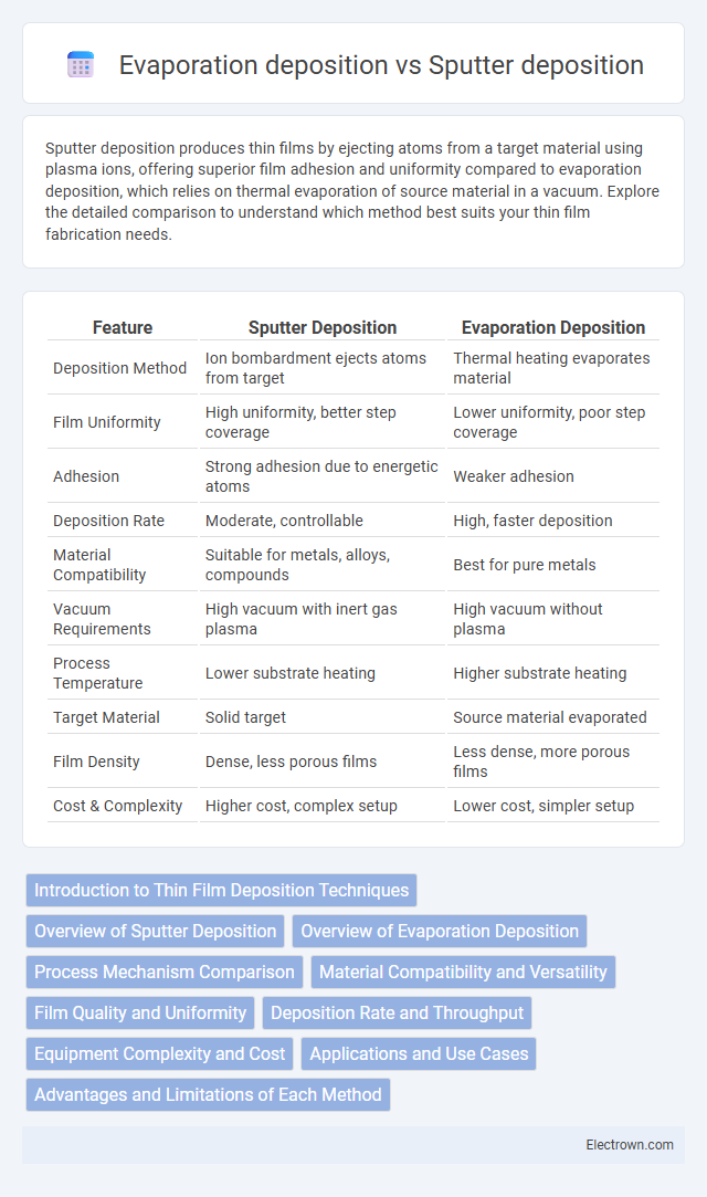
| Feature | Sputter Deposition | Evaporation Deposition |
|---|---|---|
| Deposition Method | Ion bombardment ejects atoms from target | Thermal heating evaporates material |
| Film Uniformity | High uniformity, better step coverage | Lower uniformity, poor step coverage |
| Adhesion | Strong adhesion due to energetic atoms | Weaker adhesion |
| Deposition Rate | Moderate, controllable | High, faster deposition |
| Material Compatibility | Suitable for metals, alloys, compounds | Best for pure metals |
| Vacuum Requirements | High vacuum with inert gas plasma | High vacuum without plasma |
| Process Temperature | Lower substrate heating | Higher substrate heating |
| Target Material | Solid target | Source material evaporated |
| Film Density | Dense, less porous films | Less dense, more porous films |
| Cost & Complexity | Higher cost, complex setup | Lower cost, simpler setup |
Introduction to Thin Film Deposition Techniques
Sputter deposition and evaporation deposition are two primary thin film deposition techniques used in semiconductor manufacturing and materials science. Sputter deposition involves ejecting atoms from a target material using energetic ion bombardment, creating high-quality, dense films with excellent adhesion and uniformity. Evaporation deposition relies on thermal energy to vaporize material, enabling high deposition rates and simplicity but often results in less dense films with lower adhesion compared to sputtering.
Overview of Sputter Deposition
Sputter deposition is a physical vapor deposition (PVD) technique where atoms are ejected from a solid target by ion bombardment and deposited onto a substrate, enabling the formation of thin films with excellent adhesion and uniformity. This method offers superior control over film composition and thickness compared to evaporation deposition, making it ideal for complex alloys and multilayer coatings. Your choice of sputter deposition can enhance the durability and performance of semiconductor devices, optical coatings, and magnetic films due to its dense and high-quality film characteristics.
Overview of Evaporation Deposition
Evaporation deposition is a physical vapor deposition (PVD) technique where a material is heated in a vacuum until it vaporizes and then condenses onto a substrate, forming a thin film. This method is advantageous for depositing high-purity films with precise control over thickness and composition, commonly used in semiconductor fabrication and optical coatings. Compared to sputter deposition, evaporation deposition typically operates at lower energies, resulting in less damage to sensitive substrates but may have limitations in film uniformity on complex shapes.
Process Mechanism Comparison
Sputter deposition utilizes ionized gas to eject atoms from a target material, achieving uniform thin films through a physical sputtering process, while evaporation deposition relies on heating a source material until it vaporizes and condenses onto a substrate. The sputtering mechanism offers better control over film composition and adhesion by enabling the deposition of alloys and compounds, unlike the simpler thermal evaporation method which may result in less uniformity and lower film density. Understanding these differences helps you select the ideal technique for high-precision applications requiring strong film adherence and compositional accuracy.
Material Compatibility and Versatility
Sputter deposition supports a wider range of materials, including metals, oxides, and nitrides, due to its higher energy ion bombardment process that enables uniform film growth on complex substrates. Evaporation deposition is better suited for materials with lower melting points and tends to have limitations with compound or multi-component films because it relies on thermal vaporization. Sputtering offers greater versatility in controlling film composition and thickness, making it preferred for advanced semiconductor and optical coatings.
Film Quality and Uniformity
Sputter deposition offers superior film quality and uniformity compared to evaporation deposition due to its energetic ion bombardment process, which creates dense, adherent, and defect-free thin films. Evaporation deposition often results in films with lower density and non-uniform thickness, especially on complex substrate geometries, because material is deposited primarily by line-of-sight vapor condensation. For your applications requiring consistent film morphology and precise thickness control, sputter deposition is typically the preferred method.
Deposition Rate and Throughput
Sputter deposition generally offers a lower deposition rate compared to evaporation deposition, impacting throughput in high-volume manufacturing. You can achieve faster material buildup with evaporation due to its higher deposition rate, which enhances productivity for large-area coatings. However, sputtering provides better control over film uniformity and adhesion, potentially offsetting slower throughput in precision applications.
Equipment Complexity and Cost
Sputter deposition equipment is generally more complex and expensive than evaporation deposition systems due to the need for plasma generation and precise control of ion bombardment. Evaporation deposition setups are simpler and more cost-effective, relying on thermal heating to vaporize source material, making them suitable for budget-conscious applications. You should consider sputter deposition if you require high film adhesion and uniformity despite the higher investment in equipment.
Applications and Use Cases
Sputter deposition is widely employed in semiconductor manufacturing, thin-film coatings for solar cells, and magnetic storage devices due to its ability to produce uniform, dense films even on complex substrates. Evaporation deposition is commonly used in optical coatings, microelectronics, and decorative finishes where high-purity films and smooth surfaces are crucial. Both methods serve critical roles in producing advanced electronic components, with sputtering preferred for multi-element alloys and evaporation favored for materials with low melting points.
Advantages and Limitations of Each Method
Sputter deposition offers superior film adhesion and uniformity, making it ideal for complex surfaces and thin films with precise thickness control, but it requires higher power and can cause target damage. Evaporation deposition provides higher deposition rates and simpler equipment setup, suited for materials with low melting points, yet it struggles with step coverage and film density on uneven substrates. Your choice depends on whether you prioritize film quality and conformality (sputtering) or deposition speed and cost-effectiveness (evaporation).
Sputter deposition vs Evaporation deposition Infographic