Planar transistors feature a flat structure with current flowing horizontally, while FinFETs utilize a three-dimensional fin-shaped channel to provide better control over the current and reduce leakage. Discover how these differences impact your device's performance and efficiency by reading the rest of the article.
Table of Comparison
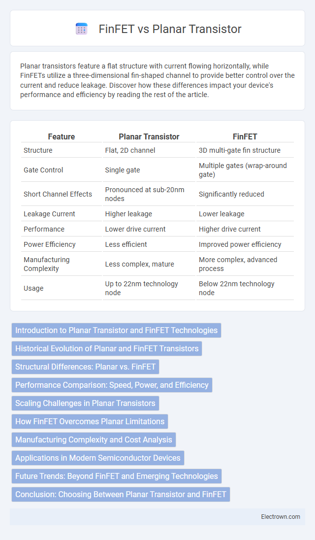
| Feature | Planar Transistor | FinFET |
|---|---|---|
| Structure | Flat, 2D channel | 3D multi-gate fin structure |
| Gate Control | Single gate | Multiple gates (wrap-around gate) |
| Short Channel Effects | Pronounced at sub-20nm nodes | Significantly reduced |
| Leakage Current | Higher leakage | Lower leakage |
| Performance | Lower drive current | Higher drive current |
| Power Efficiency | Less efficient | Improved power efficiency |
| Manufacturing Complexity | Less complex, mature | More complex, advanced process |
| Usage | Up to 22nm technology node | Below 22nm technology node |
Introduction to Planar Transistor and FinFET Technologies
Planar transistors feature a flat, two-dimensional structure where the channel lies directly beneath the gate, enabling straightforward fabrication and effective control at larger process nodes. FinFET technology introduces a three-dimensional fin-shaped channel that extends vertically from the substrate, significantly improving electrostatic control and reducing short-channel effects in advanced nodes below 20nm. The transition from planar transistors to FinFETs marked a pivotal shift in semiconductor device architecture, enabling continued scaling in CMOS technology to enhance performance and power efficiency.
Historical Evolution of Planar and FinFET Transistors
Planar transistors, developed in the 1950s, dominated semiconductor technology for decades due to their simple two-dimensional structure and ease of fabrication. The rise of FinFET transistors in the early 2010s addressed the limitations of planar designs by introducing a three-dimensional fin-shaped channel, significantly improving control over short-channel effects and enabling continued transistor scaling. This evolution marked a critical shift from traditional planar devices to advanced FinFET architectures, driving the advancement of modern high-performance and low-power integrated circuits.
Structural Differences: Planar vs. FinFET
Planar transistors feature a flat, two-dimensional channel for current flow, where the gate electrode controls the channel from above, limiting electrostatic control as device scaling continues. FinFETs utilize a three-dimensional "fin"-shaped channel that rises vertically from the substrate, enabling the gate to wrap around the fin on three sides for enhanced gate control and reduced short-channel effects. This structural difference allows FinFETs to achieve higher drive currents and improved leakage control compared to traditional planar transistor designs.
Performance Comparison: Speed, Power, and Efficiency
FinFET transistors outperform planar transistors by offering higher speed due to improved gate control and reduced short-channel effects, enabling faster switching. FinFETs exhibit lower power consumption as their 3D structure minimizes leakage currents, enhancing energy efficiency in advanced nodes. Overall, FinFET technology delivers superior performance and power efficiency compared to planar transistors, making it the preferred choice for high-performance, low-power semiconductor devices.
Scaling Challenges in Planar Transistors
Planar transistors face significant scaling challenges as channel lengths shrink below 20 nm, leading to increased short-channel effects and leakage currents. The traditional planar structure struggles with electrostatic control, causing threshold voltage variability and reduced drive current. FinFET technology overcomes these limitations by employing a 3D fin-shaped channel, enhancing gate control and enabling continued device scaling beyond the limits of planar transistors.
How FinFET Overcomes Planar Limitations
FinFET technology overcomes the electrostatic limitations of planar transistors by utilizing a three-dimensional fin-shaped channel that wraps the gate around the silicon, enhancing control over the channel and reducing leakage current. The vertical fin structure improves gate control by increasing the effective channel width and allows scaling below 22nm, where planar transistors suffer from short-channel effects and degraded performance. This architectural advancement in FinFETs results in lower power consumption, higher drive current, and improved switching speeds compared to traditional planar devices.
Manufacturing Complexity and Cost Analysis
Planar transistors feature a simpler manufacturing process with established fabrication techniques, resulting in lower production costs compared to finFETs. FinFETs require advanced 3D patterning and multiple lithography steps, increasing manufacturing complexity and capital expenditure. Your choice between planar and finFET technologies depends on balancing cost efficiency against performance gains in modern semiconductor devices.
Applications in Modern Semiconductor Devices
Planar transistors remain prevalent in low-power and analog applications due to their simpler fabrication and cost-effectiveness, especially in devices like microcontrollers and sensors. FinFET technology dominates high-performance processors and advanced mobile chipsets by offering improved control over short-channel effects, enhanced drive current, and reduced leakage power. The transition to FinFETs enables semiconductor manufacturers to push scaling beyond 14nm nodes while maintaining performance and energy efficiency in AI accelerators, GPUs, and data center CPUs.
Future Trends: Beyond FinFET and Emerging Technologies
Future trends in semiconductor technology are moving beyond FinFETs with innovations such as Gate-All-Around (GAA) transistors, which offer superior electrostatic control and scalability. Emerging technologies like nanosheet and nanowire transistors aim to overcome FinFET limitations by providing higher drive current and reduced short-channel effects. Your device performance and power efficiency will benefit as these advancements enable smaller nodes and enhanced integration in next-generation chips.
Conclusion: Choosing Between Planar Transistor and FinFET
FinFET technology offers superior control over short-channel effects, enabling enhanced performance and lower leakage currents compared to planar transistors, especially at sub-20nm nodes. Planar transistors still provide cost-effective manufacturing and simpler design for larger feature sizes, making them suitable for less demanding applications. Selecting between planar transistor and FinFET depends on the target application's performance requirements, power efficiency needs, and fabrication technology capabilities.
Planar transistor vs finFET Infographic