Split gate technology offers enhanced control over electron flow by dividing the gate into separate regions, reducing leakage current and improving device performance compared to standard gate designs. Explore the rest of this article to understand how each gate type impacts your semiconductor applications.
Table of Comparison
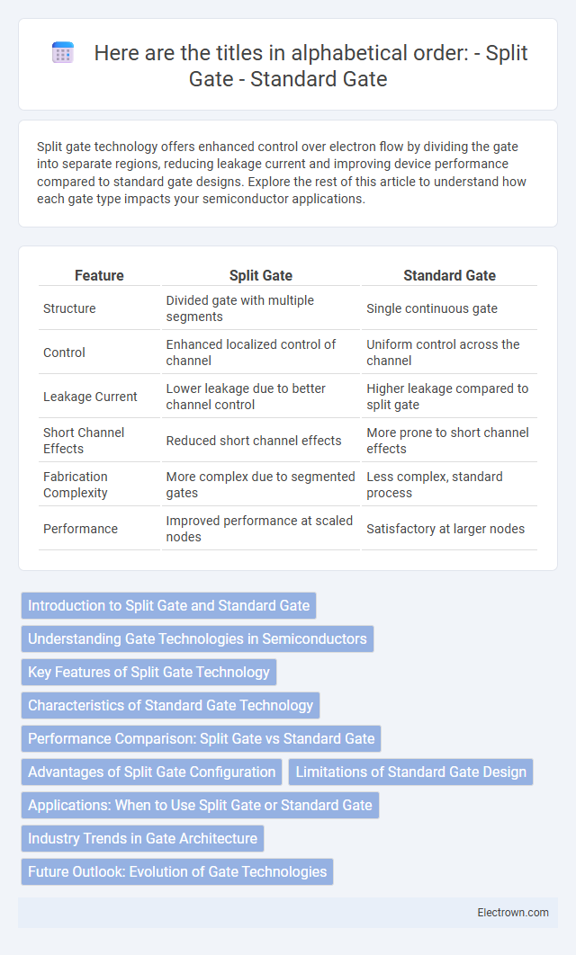
| Feature | Split Gate | Standard Gate |
|---|---|---|
| Structure | Divided gate with multiple segments | Single continuous gate |
| Control | Enhanced localized control of channel | Uniform control across the channel |
| Leakage Current | Lower leakage due to better channel control | Higher leakage compared to split gate |
| Short Channel Effects | Reduced short channel effects | More prone to short channel effects |
| Fabrication Complexity | More complex due to segmented gates | Less complex, standard process |
| Performance | Improved performance at scaled nodes | Satisfactory at larger nodes |
Introduction to Split Gate and Standard Gate
Split gate technology features two closely spaced gate electrodes that control the channel conductivity separately, enhancing electric field control and reducing short-channel effects in nanoscale transistors. Standard gate refers to a single, continuous gate electrode that modulates the entire channel uniformly but may suffer from increased leakage and reduced control as device dimensions shrink. The split gate design is increasingly used in advanced semiconductor devices to improve performance, scalability, and power efficiency compared to traditional standard gate architectures.
Understanding Gate Technologies in Semiconductors
Split gate technology in semiconductors enhances control over charge carriers by utilizing two independently biased gates, improving device performance in flash memory applications. Standard gate structures rely on a single gate electrode, offering simpler fabrication but limited control over threshold voltage and scaling. The split gate design reduces short channel effects and enhances data retention, making it preferable for advanced non-volatile memory devices.
Key Features of Split Gate Technology
Split gate technology offers enhanced charge control by incorporating a secondary gate that independently modulates the channel, leading to improved threshold voltage stability and reduced short-channel effects. The design allows for better leakage current suppression and increased drive current efficiency compared to standard gate structures. This results in superior device performance, particularly in low-power and high-speed semiconductor applications.
Characteristics of Standard Gate Technology
Standard gate technology features a conventional MOSFET structure characterized by a single control gate directly over the channel region, enabling straightforward design and fabrication processes. Its electrostatic control, while effective for many applications, may encounter limitations such as short-channel effects and increased leakage currents at nanoscale dimensions. Your choice of gate technology influences device scalability and performance, with standard gates offering cost-effective solutions but potentially less optimal control compared to advanced alternatives like split gate designs.
Performance Comparison: Split Gate vs Standard Gate
Split gate transistors offer enhanced electrostatic control and reduced short-channel effects compared to standard gate devices, resulting in improved subthreshold slope and lower leakage currents. Performance metrics such as drive current (I_on) and switching speed typically favor split gate designs due to their ability to suppress drain-induced barrier lowering (DIBL) and improve channel modulation. These advantages make split gate technology particularly suitable for low-power, high-speed applications where precise gate control directly impacts device efficiency and reliability.
Advantages of Split Gate Configuration
Split gate configuration in semiconductor devices offers enhanced control over the channel by independently biasing different gate sections, resulting in reduced short-channel effects and improved device scalability. This improved electrostatic control leads to higher drive current and lower leakage currents compared to standard gate designs. The split gate structure also enables advanced functionalities such as multi-threshold operation and reduced power consumption in modern transistor technologies.
Limitations of Standard Gate Design
Standard gate design suffers from high leakage currents and short-channel effects as transistor dimensions shrink, limiting its scalability for advanced semiconductor nodes. The lack of effective electrostatic control in standard gates contributes to increased power consumption and reduced device reliability in modern CMOS technology. These limitations have prompted the development of split gate architectures to improve gate control and reduce leakage in nanoscale transistors.
Applications: When to Use Split Gate or Standard Gate
Split gates are ideal for advanced semiconductor devices requiring precise electrostatic control, such as quantum dots and high-electron-mobility transistors (HEMTs) used in quantum computing and high-frequency applications. Standard gates are preferred in conventional CMOS technologies for general-purpose integrated circuits, where fabrication simplicity and cost-effectiveness are prioritized. Choose split gates for nanoscale electron confinement and tunable electronic properties, while standard gates suit large-scale digital and analog circuit applications.
Industry Trends in Gate Architecture
Split gate technology is gaining traction in the semiconductor industry due to its ability to reduce short-channel effects and improve device scalability compared to standard gate architectures. Industry trends show a growing adoption of split gates in advanced transistors, offering enhanced control over channel conductivity and reducing leakage currents, which drives higher performance in modern integrated circuits. Your designs can benefit from incorporating split gate structures to meet the increasing demand for energy efficiency and miniaturization in next-generation electronic devices.
Future Outlook: Evolution of Gate Technologies
Split gate technology offers enhanced control over channel formation, enabling greater power efficiency and scalability compared to standard gates. As semiconductor devices continue to shrink, split gates are expected to play a critical role in reducing leakage currents and improving device performance in advanced nodes. Your semiconductor designs may benefit from adopting split gate architectures to meet evolving demands in low-power, high-speed applications.
Split gate vs Standard gate Infographic