The drift region in semiconductor devices facilitates carrier movement under an electric field, enhancing charge transport and device performance, while the no-drift region lacks this directed carrier flow, often resulting in different electrical characteristics. Explore the article to understand how these regions impact your device's efficiency and application.
Table of Comparison
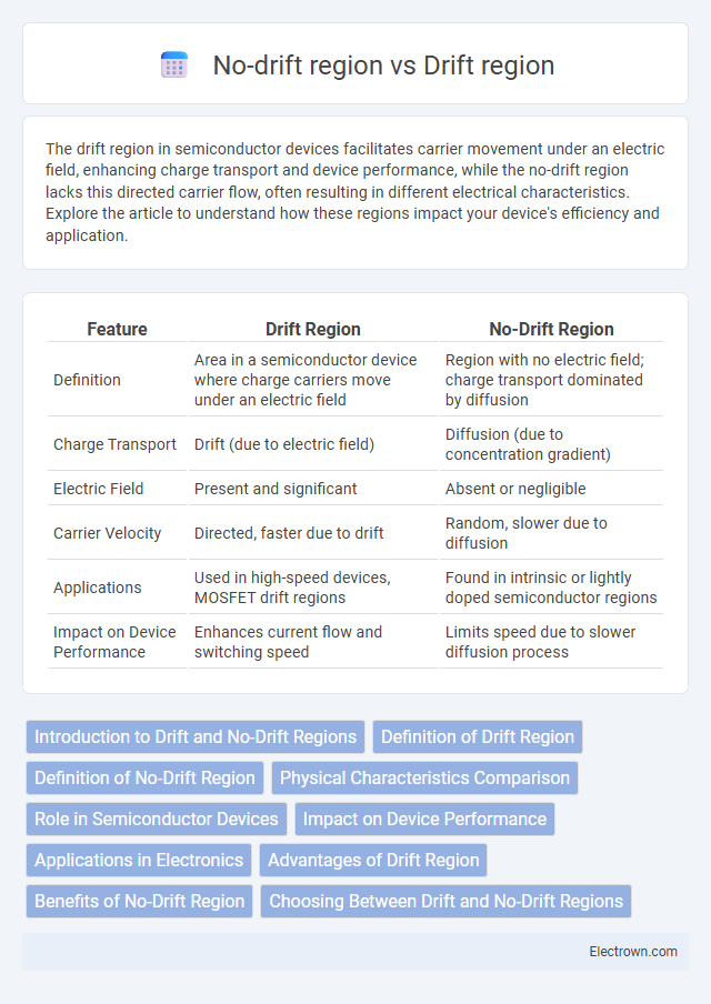
| Feature | Drift Region | No-Drift Region |
|---|---|---|
| Definition | Area in a semiconductor device where charge carriers move under an electric field | Region with no electric field; charge transport dominated by diffusion |
| Charge Transport | Drift (due to electric field) | Diffusion (due to concentration gradient) |
| Electric Field | Present and significant | Absent or negligible |
| Carrier Velocity | Directed, faster due to drift | Random, slower due to diffusion |
| Applications | Used in high-speed devices, MOSFET drift regions | Found in intrinsic or lightly doped semiconductor regions |
| Impact on Device Performance | Enhances current flow and switching speed | Limits speed due to slower diffusion process |
Introduction to Drift and No-Drift Regions
The drift region in semiconductor devices refers to the area where charge carriers move under the influence of an electric field, contributing to the device's conductivity and performance, especially in high-voltage applications. The no-drift region is characterized by minimal or no electric field, resulting in negligible carrier movement and reduced impact on current flow. Understanding the distinction between drift and no-drift regions is critical for optimizing device design, particularly in power transistors and diodes where electric field distribution governs breakdown voltage and switching speed.
Definition of Drift Region
The drift region in semiconductor devices refers to a lightly doped area where carriers are accelerated by an electric field, enabling charge transport over a distance without frequent recombination. This region is crucial for supporting high voltage in power devices, as it controls the device's breakdown voltage and affects on-resistance. Understanding your device's drift region characteristics helps optimize performance in high-power and high-frequency applications.
Definition of No-Drift Region
The no-drift region refers to the area in a semiconductor device where charge carriers move primarily by diffusion rather than drift due to the absence or minimal influence of an electric field. In contrast, the drift region is characterized by carrier movement driven mainly by the electric field applied across the device. Understanding the no-drift region is crucial for analyzing charge transport mechanisms in devices such as diodes and transistors, impacting their electrical characteristics and performance.
Physical Characteristics Comparison
The drift region in semiconductor devices is characterized by a lightly doped, extended area designed to sustain high voltage and control the electric field distribution, whereas the no-drift region features a heavily doped, compact structure that enhances current conduction but limits voltage handling. The physical length and doping concentration in the drift region directly influence device breakdown voltage and on-resistance, while the no-drift region prioritizes minimal resistance for efficient current flow. Understanding these physical characteristics helps you optimize device performance for high-voltage or high-speed applications.
Role in Semiconductor Devices
The drift region in semiconductor devices plays a crucial role in establishing an electric field that enables charge carriers to move under the influence of voltage, thus facilitating controlled current flow and device switching. In contrast, the no-drift region lacks such an electric field, relying primarily on diffusion to move carriers, which results in slower conduction and less precise control. This distinction impacts device performance metrics such as response time, power efficiency, and breakdown voltage tolerance in components like diodes and transistors.
Impact on Device Performance
The drift region in semiconductor devices significantly affects device performance by controlling the electric field distribution and breakdown voltage, enabling higher voltage operation and improved reliability. Devices without a drift region typically exhibit lower on-resistance but suffer from reduced voltage handling capability, limiting their use in high-power applications. Optimizing the drift region length and doping concentration directly enhances your device's efficiency by balancing conduction losses and voltage endurance.
Applications in Electronics
Drift regions play a crucial role in power devices such as MOSFETs and IGBTs, enabling efficient voltage blocking and current conduction by supporting high electric fields, which is essential for high-power applications. No-drift regions are typically found in low-power, high-speed devices where minimal resistance and capacitance are critical for fast switching and signal integrity, such as in digital integrated circuits. Understanding the impact of drift and no-drift regions helps optimize your electronic designs for specific applications, balancing efficiency and performance requirements.
Advantages of Drift Region
The drift region in semiconductor devices enhances voltage blocking capability by increasing the breakdown voltage without compromising on on-state resistance. It enables efficient charge carrier transport under high electric fields, improving device performance in high-voltage applications such as power diodes and MOSFETs. This region also contributes to lower power losses and better thermal stability compared to no-drift region designs.
Benefits of No-Drift Region
The no-drift region eliminates carrier transit delays, significantly improving switching speed and frequency response in semiconductor devices. Reduced power loss and lower on-resistance enhance overall efficiency and thermal management, making it ideal for high-performance power electronics. The compact structure also enables smaller device footprints, contributing to cost-effective and scalable designs.
Choosing Between Drift and No-Drift Regions
When choosing between drift and no-drift regions in semiconductor devices, consider the trade-off between breakdown voltage and on-resistance. Drift regions increase breakdown voltage by extending the depletion region but add resistance, impacting device efficiency. Your design should balance these factors to optimize performance for high-voltage or high-speed applications.
Drift region vs no-drift region Infographic