Diffused junctions are created by introducing impurities into a semiconductor substrate through diffusion, resulting in a gradual impurity concentration profile, while planar junctions are formed using photolithography and etching techniques, producing a well-defined, flat junction with precise control over dimensions. Understanding the differences between diffused and planar junctions can help you choose the right semiconductor technology for your specific application; explore the rest of the article to learn more.
Table of Comparison
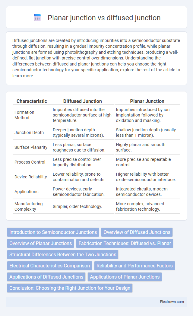
| Characteristic | Diffused Junction | Planar Junction |
|---|---|---|
| Formation Method | Impurities diffused into the semiconductor surface at high temperature. | Impurities introduced by ion implantation followed by oxidation and masking. |
| Junction Depth | Deeper junction depth (typically several microns). | Shallow junction depth (usually less than 1 micron). |
| Surface Planarity | Less planar, surface roughness due to diffusion. | Highly planar and smooth surface. |
| Process Control | Less precise control over impurity distribution. | More precise and repeatable control. |
| Device Reliability | Lower reliability, prone to contamination and defects. | Higher reliability with better oxide-semiconductor interface. |
| Applications | Power devices, early semiconductor fabrication. | Integrated circuits, modern semiconductor devices. |
| Manufacturing Complexity | Simpler, older technology. | More complex, advanced fabrication technology. |
Introduction to Semiconductor Junctions
Semiconductor junctions, fundamental to electronic devices, include diffused and planar types, each formed through distinct fabrication methods influencing device performance. Diffused junctions arise from high-temperature diffusion of dopants into the semiconductor substrate, creating graded impurity profiles that affect carrier concentration and electric field distribution. Planar junctions are manufactured using thin film and photolithographic techniques resulting in abrupt junctions with precise control over dopant placement, enhancing reliability and enabling higher-density integration in modern integrated circuits.
Overview of Diffused Junctions
Diffused junctions are created by introducing dopants into a semiconductor substrate through high-temperature diffusion, resulting in a gradual concentration gradient of impurities. This process produces a smooth, non-abrupt transition between p-type and n-type regions, which enhances device reliability and reduces junction breakdown risks. Diffused junctions are commonly used in bipolar junction transistors and diodes where precise control over doping profiles is essential for optimal electrical performance.
Overview of Planar Junctions
Planar junctions are semiconductor interfaces fabricated using photolithographic techniques to create precise, flat surfaces essential for integrated circuit manufacturing. Unlike diffused junctions that involve doping impurities deeper into the substrate, planar junctions maintain shallow, well-defined junction depths, enhancing device performance and reliability. This method significantly improves control over junction profiles, reduces leakage currents, and allows for scalable production in modern microelectronics.
Fabrication Techniques: Diffused vs. Planar
Diffused junctions are created by introducing dopants into the semiconductor substrate through high-temperature thermal diffusion, allowing atoms to penetrate the surface and form a PN junction, resulting in a gradual doping profile. Planar junctions utilize oxidation to form a silicon dioxide mask on the wafer surface, followed by photolithography and ion implantation for precise and localized doping, producing sharp junctions with improved control over depth and concentration. The planar process offers superior scalability and integration capabilities compared to diffused junctions due to its compatibility with modern semiconductor fabrication and high-resolution patterning.
Structural Differences Between the Two Junctions
Diffused junctions are formed by introducing impurities through thermal diffusion, resulting in a gradual concentration gradient and a deep, rounded junction profile. Planar junctions utilize photolithographic techniques to create sharp, flat interfaces with precise control over junction depth and uniformity. Your choice between these structures impacts device performance, with planar junctions offering better scalability and integration for modern semiconductor devices.
Electrical Characteristics Comparison
Diffused junctions typically exhibit higher series resistance and increased junction capacitance due to deeper impurity penetration, impacting high-frequency performance negatively compared to planar junctions. Planar junctions offer superior electrical characteristics with lower leakage currents and enhanced breakdown voltage, resulting from their shallow junction depths and better surface passivation. Your circuit performance can significantly improve by choosing planar junction devices where low noise and fast switching are critical.
Reliability and Performance Factors
Diffused junctions offer superior reliability due to their gradual impurity profiles, which reduce electric field gradients and minimize the risk of junction breakdown, enhancing overall device stability. Planar junctions provide improved performance with precise control over junction depth and doping concentration, resulting in higher speed and lower leakage currents in integrated circuits. Both junction types balance reliability and performance by optimizing impurity distribution and manufacturing techniques suited for specific semiconductor applications.
Applications of Diffused Junctions
Diffused junctions are widely utilized in power semiconductor devices such as diodes and transistors due to their ability to form precise and controlled doping profiles, enhancing device performance in high-voltage and high-current applications. Their fabrication process supports better thermal stability and junction depth control, making them suitable for integrated circuits in analog and digital electronics. Understanding the advantages of diffused junctions can help you optimize semiconductor device designs for reliability and efficiency.
Applications of Planar Junctions
Planar junctions are widely used in integrated circuit fabrication due to their precise control over junction depth and doping profiles, enabling high-performance semiconductor devices like MOSFETs and BJTs. Their planar structure allows for scalable manufacturing processes essential in microelectronics and VLSI technology. This junction type supports advanced applications in analog and digital circuits, power devices, and sensor technology, ensuring improved reliability and device miniaturization.
Conclusion: Choosing the Right Junction for Your Design
Diffused junctions offer simplicity and cost-effectiveness for low-power, low-frequency applications, while planar junctions provide superior performance, higher reliability, and better control in high-frequency and integrated circuit designs. Selecting the right junction depends on specific design requirements such as thermal stability, junction capacitance, and manufacturing complexity. Engineers prioritize planar junctions in modern semiconductor fabrication due to their optimized electrical characteristics and scalability for advanced applications.
Diffused junction vs planar junction Infographic