Phase-shift masks enhance lithography resolution by manipulating light phase to improve edge definition, while binary masks rely solely on opaque patterns to block light. Explore the rest of the article to understand which mask technology suits your semiconductor manufacturing needs.
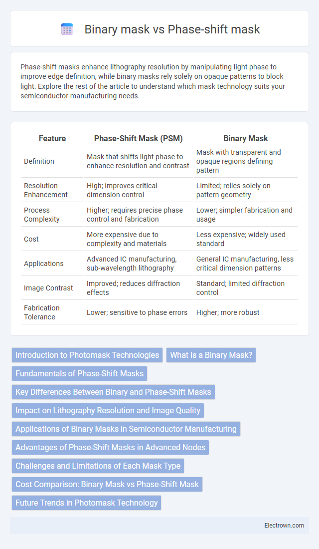
Table of Comparison
| Feature | Phase-Shift Mask (PSM) | Binary Mask |
|---|---|---|
| Definition | Mask that shifts light phase to enhance resolution and contrast | Mask with transparent and opaque regions defining pattern |
| Resolution Enhancement | High; improves critical dimension control | Limited; relies solely on pattern geometry |
| Process Complexity | Higher; requires precise phase control and fabrication | Lower; simpler fabrication and usage |
| Cost | More expensive due to complexity and materials | Less expensive; widely used standard |
| Applications | Advanced IC manufacturing, sub-wavelength lithography | General IC manufacturing, less critical dimension patterns |
| Image Contrast | Improved; reduces diffraction effects | Standard; limited diffraction control |
| Fabrication Tolerance | Lower; sensitive to phase errors | Higher; more robust |
Introduction to Photomask Technologies
Phase-shift masks enhance photolithography resolution by modulating the light phase to improve image contrast, offering superior pattern fidelity compared to traditional binary masks that solely block or transmit light. These advanced masks are crucial in semiconductor manufacturing processes where feature sizes continue to shrink below the wavelength of light, enabling the fabrication of integrated circuits with higher density and performance. Understanding the differences between phase-shift and binary masks is essential for optimizing photomask design and achieving precise pattern transfer on silicon wafers.
What is a Binary Mask?
A binary mask in photolithography is a type of photomask that uses two distinct levels of opacity to create clear, defined patterns on a semiconductor wafer. It operates by blocking or transmitting light through transparent and opaque regions, making it ideal for straightforward patterning tasks. Your choice of a binary mask affects resolution and depth of focus, especially compared to more advanced phase-shift masks used for finer feature control.
Fundamentals of Phase-Shift Masks
Phase-shift masks (PSMs) enhance photolithography resolution by modifying the phase of light passing through the mask, allowing interference effects to sharpen image edges on the wafer. Unlike binary masks that use opaque and transparent regions to block or transmit light, PSMs introduce a phase difference, typically 180 degrees, between adjacent areas to improve feature contrast beyond the diffraction limit. Your semiconductor fabrication process benefits from PSM technology through increased pattern fidelity and the ability to achieve smaller critical dimensions compared to traditional binary masks.
Key Differences Between Binary and Phase-Shift Masks
Binary masks use opaque and transparent regions to define circuit patterns, whereas phase-shift masks manipulate the phase of light waves to enhance resolution and contrast. Phase-shift masks enable finer feature printing by creating destructive interference, leading to improved lithographic precision compared to the simpler binary masks. This technology is crucial for advanced semiconductor manufacturing processes at sub-wavelength scales, offering higher image fidelity and critical dimension control.
Impact on Lithography Resolution and Image Quality
Phase-shift masks significantly enhance lithography resolution by manipulating the phase of light waves, enabling finer pattern printing below the diffraction limit compared to binary masks that rely solely on opacity differences. This phase modulation reduces image blur and increases pattern contrast, resulting in higher image quality and improved critical dimension control. Binary masks, while simpler and cost-effective, often suffer from lower resolution and diminished image fidelity due to weaker light modulation capabilities.
Applications of Binary Masks in Semiconductor Manufacturing
Binary masks are widely used in semiconductor manufacturing for patterning integrated circuits due to their simplicity and cost-effectiveness in photolithography processes. These masks enable precise transfer of circuit designs onto silicon wafers, facilitating the mass production of microchips with high resolution and repeatability. They are particularly effective in fabricating standard IC layers where complex phase-shift techniques are unnecessary.
Advantages of Phase-Shift Masks in Advanced Nodes
Phase-shift masks (PSMs) offer superior resolution and depth of focus compared to binary masks, enabling critical feature sizes below 100 nm in advanced semiconductor nodes. They enhance pattern fidelity by manipulating light phase, reducing diffraction effects and improving process window margins, which is crucial for sub-7nm technology. If you're working on cutting-edge IC fabrication, leveraging PSM technology boosts yield and device performance by enabling finer, more accurate patterning.
Challenges and Limitations of Each Mask Type
Phase-shift masks (PSM) offer superior resolution enhancement compared to binary masks but face challenges such as increased complexity in design and fabrication, leading to higher production costs and potential defects. Binary masks are simpler and more cost-effective but often suffer from limited resolution capabilities and insufficient control over light diffraction, restricting their use in advanced lithography processes. Your choice between these masks should consider the trade-off between resolution needs and manufacturing precision constraints inherent to each type.
Cost Comparison: Binary Mask vs Phase-Shift Mask
Phase-shift masks generally incur higher manufacturing costs than binary masks due to their complex design and precision etching requirements. Binary masks are more cost-effective for high-volume production as they involve simpler fabrication processes and lower material expenses. Your choice between these masks should consider budget constraints alongside process performance needs, as phase-shift masks can justify their cost through improved resolution and pattern fidelity in advanced lithography.
Future Trends in Photomask Technology
Phase-shift masks (PSM) offer enhanced resolution and improved depth of focus compared to binary masks, enabling semiconductor manufacturers to meet the demand for smaller feature sizes in advanced nodes. Future trends in photomask technology emphasize integrating hybrid mask strategies combining PSM and binary masks to optimize cost and performance in extreme ultraviolet lithography (EUV) and deep ultraviolet (DUV) applications. Emerging developments include the adoption of computational lithography techniques and machine learning algorithms to enhance mask design accuracy and defect detection, driving the next generation of photomask innovation.
Phase-shift mask vs binary mask Infographic