CMOS latch-up occurs when a parasitic thyristor in traditional bulk CMOS triggers a low-resistance path, causing device failure, while SOI (Silicon-On-Insulator) technology inherently reduces latch-up risk due to its insulating layer that isolates devices from the substrate. Understanding these differences is crucial for your circuit design reliability, so continue reading to explore detailed comparisons and prevention techniques.
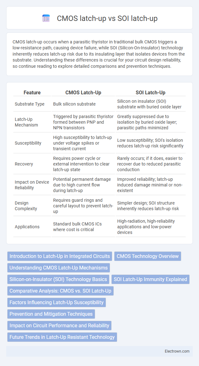
Table of Comparison
| Feature | CMOS Latch-Up | SOI Latch-Up |
|---|---|---|
| Substrate Type | Bulk silicon substrate | Silicon on insulator (SOI) substrate with buried oxide layer |
| Latch-Up Mechanism | Triggered by parasitic thyristor formed between PNP and NPN transistors | Greatly suppressed due to isolation by buried oxide layer; parasitic paths minimized |
| Susceptibility | High susceptibility to latch-up under voltage spikes or transient current | Low susceptibility; SOI's isolation reduces latch-up risk significantly |
| Recovery | Requires power cycle or external intervention to clear latch-up state | Rarely occurs; if it does, easier to recover due to reduced parasitic conduction |
| Impact on Device Reliability | Potential permanent damage due to high current flow during latch-up | Improved reliability; latch-up induced damage minimal or non-existent |
| Design Complexity | Requires guard rings and careful layout to prevent latch-up | Simpler design; SOI structure inherently reduces latch-up risk |
| Applications | Standard bulk CMOS ICs where cost is critical | High-radiation, high-reliability applications and low-power devices |
Introduction to Latch-Up in Integrated Circuits
Latch-up in integrated circuits occurs when parasitic thyristor structures create a low-impedance path, causing high current and potential device failure. CMOS latch-up is typically triggered by substrate injection and involves the silicon bulk, leading to significant power dissipation and device degradation. In contrast, SOI latch-up is less common due to the buried oxide layer electrically isolating the device, reducing parasitic current paths and enhancing latch-up immunity in SOI-based integrated circuits.
CMOS Technology Overview
CMOS technology, widely used in integrated circuits, relies on complementary pairs of p-type and n-type MOSFETs to achieve low power consumption and high noise immunity. In bulk CMOS, latch-up occurs due to parasitic thyristor structures formed between the p-well and n-well regions, causing a short circuit that can damage the device. SOI (Silicon-On-Insulator) technology mitigates latch-up by isolating transistors with a buried oxide layer, significantly reducing parasitic interactions and improving device reliability.
Understanding CMOS Latch-Up Mechanisms
CMOS latch-up occurs when parasitic PNPN structures within the silicon substrate create a low-impedance path, leading to high current flow and potential device failure. SOI (Silicon-On-Insulator) technology reduces latch-up risk by isolating the active silicon layer with an insulator, effectively interrupting the parasitic thyristor paths. Understanding these mechanisms helps you design more robust circuits by selecting appropriate fabrication processes to minimize latch-up susceptibility.
Silicon-on-Insulator (SOI) Technology Basics
Silicon-on-Insulator (SOI) technology reduces latch-up susceptibility by incorporating a buried oxide layer that electrically isolates the transistor body from the substrate, unlike bulk CMOS where the substrate acts as a common path for parasitic current flow. This insulating layer minimizes parasitic thyristor formation responsible for latch-up in traditional CMOS circuits, enhancing robustness against high-voltage transients. Your integrated circuits benefit from SOI's intrinsic latch-up immunity, improving reliability and performance in harsh electronic environments.
SOI Latch-Up Immunity Explained
SOI latch-up immunity is primarily due to the insulated buried oxide layer in Silicon-On-Insulator technology, which effectively isolates the transistor body from the substrate, preventing parasitic thyristor formation. In contrast, conventional CMOS on bulk silicon is susceptible to latch-up because the p-n-p-n structure enables a parasitic SCR, causing a low-impedance path and potential device failure. The inherent electrical isolation provided by the SOI substrate significantly enhances latch-up robustness, making SOI devices ideal for high-reliability and radiation-hardened applications.
Comparative Analysis: CMOS vs. SOI Latch-Up
CMOS latch-up occurs due to parasitic thyristor action in bulk silicon, causing high current and potential device failure, while SOI latch-up is significantly reduced because the buried oxide layer suppresses parasitic conduction paths. The intrinsic isolation in SOI technology minimizes substrate coupling and enhances latch-up immunity, making it more reliable in high-density integrated circuits. Understanding these differences helps you select the appropriate technology for robust circuit design in environments prone to latch-up events.
Factors Influencing Latch-Up Susceptibility
Latch-up susceptibility in CMOS technology is primarily influenced by factors such as substrate doping concentration, well design, and the presence of parasitic thyristor structures, which facilitate unintended current paths under stress conditions. In contrast, SOI (Silicon-On-Insulator) technology significantly reduces latch-up risk due to the buried oxide layer that electrically isolates the active silicon film from the bulk substrate, effectively suppressing parasitic bipolar action. Additionally, thermal effects, supply voltage levels, and layout techniques also play critical roles in determining latch-up susceptibility in both CMOS and SOI devices.
Prevention and Mitigation Techniques
CMOS latch-up prevention techniques include well-tied substrates, guard rings, and optimized layout spacing to reduce parasitic transistor activation, while SOI latch-up is inherently minimized due to the insulating buried oxide layer preventing substrate current paths. In SOI technology, latch-up mitigation focuses on minimizing floating body effects through body contact engineering and advanced biasing schemes, ensuring device stability without complex substrate ties. Your design can benefit from selecting SOI for environments where latch-up is critical, leveraging its intrinsic isolation alongside careful device and layout optimization to reduce latch-up risk effectively.
Impact on Circuit Performance and Reliability
CMOS latch-up significantly degrades circuit performance by causing high current spikes that can lead to device failure and reduced reliability due to increased susceptibility to parasitic thyristor triggering. SOI (Silicon-On-Insulator) technology drastically improves latch-up immunity by electrically isolating transistors with a buried oxide layer, minimizing parasitic interactions and thereby enhancing circuit reliability and stability. The intrinsic latch-up resistance in SOI circuits results in superior operational longevity and consistent performance in high-density and high-speed integrated circuits.
Future Trends in Latch-Up Resistant Technology
Emerging trends in latch-up resistant technology emphasize reduced susceptibility in SOI (Silicon-On-Insulator) devices compared to traditional bulk CMOS, due to their inherent isolation layers that minimize parasitic thyristor formation. Advances in SOI semiconductor processes enhance latch-up immunity, enabling higher density and lower power designs for future integrated circuits. Your choice of SOI technology can significantly improve latch-up robustness, facilitating more reliable and scalable electronics in next-generation applications.
CMOS latch-up vs SOI latch-up Infographic