Epitaxial wafers feature a thin, high-purity crystalline layer grown atop a bulk wafer, enhancing electrical performance and device uniformity compared to traditional bulk wafers composed of a single homogeneous crystal. Discover how choosing between epitaxial and bulk wafers can impact your semiconductor manufacturing process in the rest of this article.
Table of Comparison
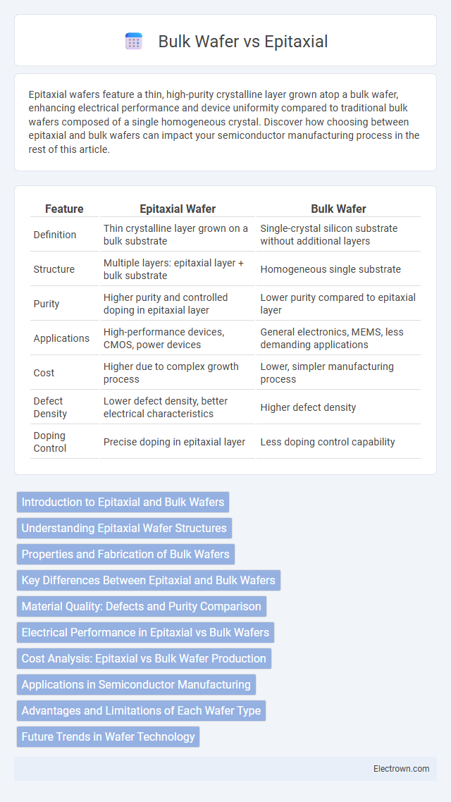
| Feature | Epitaxial Wafer | Bulk Wafer |
|---|---|---|
| Definition | Thin crystalline layer grown on a bulk substrate | Single-crystal silicon substrate without additional layers |
| Structure | Multiple layers: epitaxial layer + bulk substrate | Homogeneous single substrate |
| Purity | Higher purity and controlled doping in epitaxial layer | Lower purity compared to epitaxial layer |
| Applications | High-performance devices, CMOS, power devices | General electronics, MEMS, less demanding applications |
| Cost | Higher due to complex growth process | Lower, simpler manufacturing process |
| Defect Density | Lower defect density, better electrical characteristics | Higher defect density |
| Doping Control | Precise doping in epitaxial layer | Less doping control capability |
Introduction to Epitaxial and Bulk Wafers
Epitaxial wafers consist of a thin, single-crystal silicon layer grown on a bulk silicon substrate, providing enhanced control over electrical properties and reduced defects for semiconductor device fabrication. Bulk wafers are made from a single, solid silicon crystal, offering consistency and cost-effectiveness but lacking the specialized surface layer found in epitaxial wafers. The choice between epitaxial and bulk wafers significantly impacts the performance, yield, and application of integrated circuits in microelectronics.
Understanding Epitaxial Wafer Structures
Epitaxial wafer structures consist of a thin, highly controlled silicon layer grown atop a bulk silicon substrate, enabling precise electrical properties and enhanced device performance. Your semiconductor designs benefit from improved uniformity, reduced defect density, and better dopant control compared to traditional bulk wafers. This distinct layering technique is essential for advanced integrated circuits and power devices requiring high reliability and efficiency.
Properties and Fabrication of Bulk Wafers
Bulk wafers are fabricated from a single crystal ingot grown using methods like Czochralski or Float Zone, ensuring high purity and uniform crystal structure throughout the wafer. Their properties include excellent mechanical strength, thermal conductivity, and electrical characteristics, making them ideal for various semiconductor applications. Bulk wafer fabrication emphasizes control over doping concentration and wafer thickness to meet specific device requirements.
Key Differences Between Epitaxial and Bulk Wafers
Epitaxial wafers feature a thin, single-crystal silicon layer grown atop a bulk silicon substrate, enhancing electrical characteristics and enabling precise control over doping concentrations. Bulk wafers consist entirely of a single crystal silicon substrate without additional epitaxial layers, offering cost-effective manufacturing but less control over surface properties. The primary differences lie in the epitaxial layer's uniformity, reduced defect density, and improved device performance compared to the homogeneous structure of bulk wafers.
Material Quality: Defects and Purity Comparison
Epitaxial wafers exhibit superior material quality with significantly lower defect densities and higher purity levels compared to bulk wafers, as the thin epitaxial layer is grown on a highly controlled substrate, minimizing impurities and crystalline imperfections. Bulk wafers often contain more intrinsic defects due to their single-crystal growth process, which can introduce dislocations and residual stresses affecting electronic performance. Your semiconductor devices benefit from the enhanced electrical properties and reliability offered by epitaxial wafers through their optimized defect control and material purity.
Electrical Performance in Epitaxial vs Bulk Wafers
Epitaxial wafers exhibit superior electrical performance compared to bulk wafers due to their highly controlled doping concentration and reduced defect density, which enhance carrier mobility and reduce leakage currents. The epitaxial layer provides a uniform, defect-free semiconductor surface ideal for high-speed and low-noise devices, whereas bulk wafers often suffer from higher impurity levels and crystal imperfections. This results in improved device reliability, faster switching speeds, and lower power consumption for epitaxial-based integrated circuits.
Cost Analysis: Epitaxial vs Bulk Wafer Production
Epitaxial wafer production involves higher manufacturing costs due to complex layer deposition processes and stringent purity requirements compared to bulk wafers, which are produced directly from single crystal silicon ingots at lower expenses. The cost difference impacts your semiconductor project budgets, as epitaxial wafers offer enhanced electrical properties but require more advanced equipment and longer processing times. Bulk wafers provide a cost-effective solution for standard applications where ultra-high purity or precise layer thickness is not critical.
Applications in Semiconductor Manufacturing
Epitaxial wafers are critical in semiconductor manufacturing for high-performance devices such as advanced integrated circuits, power devices, and radio-frequency components due to their controlled thickness and superior crystal quality. Bulk wafers are commonly used in general semiconductor applications where cost-efficiency and mechanical robustness are essential, such as in memory chips and standard logic devices. Your choice between epitaxial and bulk wafers directly impacts device performance, yield, and manufacturing complexity in semiconductor fabrication processes.
Advantages and Limitations of Each Wafer Type
Epitaxial wafers offer superior electrical properties and uniformity due to their precisely controlled thin semiconductor layers, enhancing device performance in high-speed and high-power applications. Bulk wafers provide cost-effective substrate solutions with robust mechanical strength, making them favorable for large-scale production and simpler device structures. Limitations of epitaxial wafers include higher manufacturing costs and complexity, while bulk wafers suffer from less control over surface defects and lower electrical quality.
Future Trends in Wafer Technology
Future trends in wafer technology emphasize the growing adoption of epitaxial wafers due to their superior electrical performance, reduced defect density, and enhanced device scaling capabilities compared to traditional bulk wafers. Innovations in epitaxial growth techniques, such as atomic layer epitaxy and selective area epitaxy, enable precise control over layer thickness and composition, supporting advanced semiconductor applications like high-frequency devices and power electronics. Increasing demand for 5G infrastructure, electric vehicles, and AI-driven technologies drives the shift toward epitaxial wafers, promoting higher efficiency and smaller device footprints in next-generation integrated circuits.
Epitaxial vs bulk wafer Infographic