A CMOS inverter uses complementary p-type and n-type MOSFETs to achieve low power consumption and high noise immunity, while an NMOS inverter relies solely on NMOS transistors, resulting in higher power dissipation and slower switching speeds. Discover how these differences impact Your circuit design and performance by reading the rest of the article.
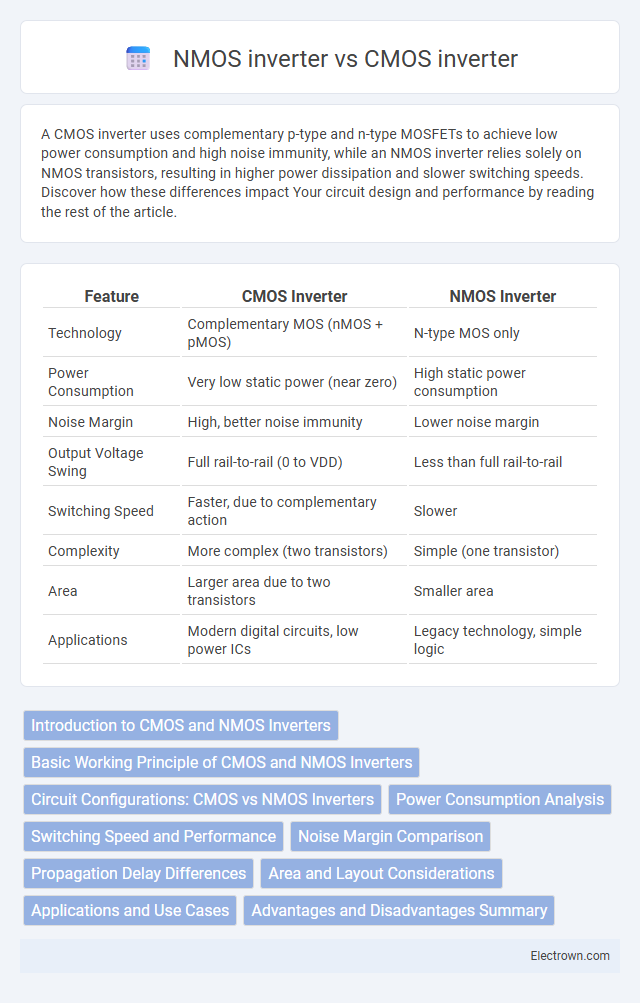
Table of Comparison
| Feature | CMOS Inverter | NMOS Inverter |
|---|---|---|
| Technology | Complementary MOS (nMOS + pMOS) | N-type MOS only |
| Power Consumption | Very low static power (near zero) | High static power consumption |
| Noise Margin | High, better noise immunity | Lower noise margin |
| Output Voltage Swing | Full rail-to-rail (0 to VDD) | Less than full rail-to-rail |
| Switching Speed | Faster, due to complementary action | Slower |
| Complexity | More complex (two transistors) | Simple (one transistor) |
| Area | Larger area due to two transistors | Smaller area |
| Applications | Modern digital circuits, low power ICs | Legacy technology, simple logic |
Introduction to CMOS and NMOS Inverters
CMOS inverters consist of complementary p-type and n-type MOSFETs, delivering high noise margins and low static power consumption due to near-zero leakage current when in steady states. NMOS inverters use only n-type MOSFETs with a resistive load, resulting in higher power dissipation and lower voltage swing compared to CMOS designs. CMOS inverter technology dominates modern digital circuits for its energy efficiency and superior switching performance versus NMOS inverter counterparts.
Basic Working Principle of CMOS and NMOS Inverters
The CMOS inverter operates using complementary pairs of p-type and n-type MOSFETs, where the pMOS transistor conducts when the input is low and the nMOS transistor conducts when the input is high, ensuring low static power consumption and full voltage swing. In contrast, the NMOS inverter relies solely on an n-type MOSFET and a load resistor, causing continuous current flow when the transistor is on, leading to higher power dissipation and less efficient switching. The CMOS inverter's efficient pull-up and pull-down network creates sharper transition characteristics compared to the NMOS inverter's resistive load, making CMOS preferable for modern low-power digital circuits.
Circuit Configurations: CMOS vs NMOS Inverters
CMOS inverter circuit configuration consists of complementary p-channel and n-channel MOSFETs connected in a push-pull arrangement, enabling low static power consumption and high noise margins. NMOS inverter design uses a single n-channel MOSFET with a passive load resistor or transistor, resulting in higher static power dissipation and lower switching speed. The CMOS configuration achieves full rail-to-rail output voltage swing, while the NMOS inverter output voltage is limited by voltage loss across the load element.
Power Consumption Analysis
CMOS inverters exhibit significantly lower power consumption compared to NMOS inverters due to their complementary transistor arrangement that minimizes static power dissipation. CMOS technology reduces direct current flow by ensuring that at least one transistor is off during switching, leading to negligible static power consumption and only dynamic power usage during transitions. In contrast, NMOS inverters suffer from continuous static current flow through the pull-down network, resulting in higher power consumption and lower energy efficiency in digital circuits.
Switching Speed and Performance
CMOS inverters exhibit significantly faster switching speeds and higher performance compared to NMOS inverters due to their complementary use of both p-type and n-type MOSFETs, which reduces power consumption and enhances voltage swing. NMOS inverters suffer from slower propagation delay and increased power dissipation because they rely solely on n-type transistors and resistive loads. The improved switching characteristics of CMOS technology make it the preferred choice for high-speed digital circuits and complex integrated systems.
Noise Margin Comparison
CMOS inverters exhibit superior noise margin compared to NMOS inverters due to their complementary transistor design, which ensures full rail-to-rail output voltage swing and reduced static power consumption. The noise margin of a CMOS inverter typically ranges between 45% to 55% of the supply voltage, while NMOS inverters have lower noise margins limited by threshold voltage drops and incomplete voltage swings. Your choice of inverter impacts circuit robustness, with CMOS providing enhanced noise immunity in digital logic applications.
Propagation Delay Differences
CMOS inverters exhibit significantly lower propagation delay compared to NMOS inverters due to their complementary transistor configuration, which ensures faster switching and reduced power loss. NMOS inverters suffer from slower response times because the pull-up load is typically a resistor or depletion-mode transistor, causing higher delays. The reduced capacitance and efficient current drive of CMOS technology directly minimize propagation delay, enhancing overall circuit speed.
Area and Layout Considerations
CMOS inverters occupy less silicon area than NMOS inverters due to their complementary transistor arrangement, which reduces static power dissipation and allows for denser circuit layouts. The symmetrical design of CMOS transistors simplifies routing and minimizes parasitic capacitances, enhancing overall layout efficiency compared to the single-transistor NMOS inverter. When optimizing your integrated circuit design, choosing CMOS inverters supports compactness and improved performance in area-constrained applications.
Applications and Use Cases
CMOS inverters are widely used in digital integrated circuits due to their low power consumption and high noise immunity, making them ideal for microprocessors, memory devices, and high-speed logic circuits. NMOS inverters, while simpler and faster in switching, are primarily applied in less power-sensitive environments such as certain analog circuits and simple digital logic where higher power consumption is acceptable. CMOS technology dominates modern electronic devices because its efficient power usage extends battery life in portable applications and reduces heat generation in large-scale integrated circuits.
Advantages and Disadvantages Summary
CMOS inverters offer low power consumption, high noise immunity, and full voltage swing output, making them ideal for modern digital circuits, but require more transistors and complex fabrication. NMOS inverters provide simpler design with faster switching speeds and lower cost, yet suffer from higher static power dissipation, limited output voltage swing, and reduced noise margins. CMOS technology dominates in integrated circuit design due to its efficiency and reliability despite its greater complexity compared to NMOS.
CMOS inverter vs NMOS inverter Infographic