Source-drain engineering focuses on optimizing the regions where current enters and exits the transistor to reduce resistance and improve overall device performance. Channel engineering involves modifying the transistor's channel properties to enhance carrier mobility and control short-channel effects; explore the rest of the article to understand how these strategies complement each other for superior semiconductor device design.
Table of Comparison
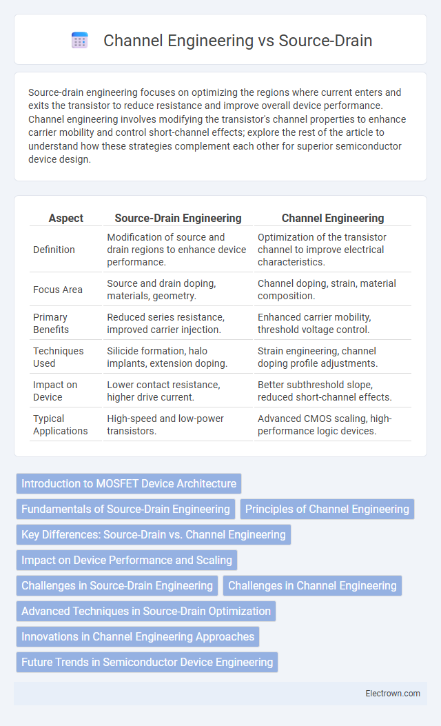
| Aspect | Source-Drain Engineering | Channel Engineering |
|---|---|---|
| Definition | Modification of source and drain regions to enhance device performance. | Optimization of the transistor channel to improve electrical characteristics. |
| Focus Area | Source and drain doping, materials, geometry. | Channel doping, strain, material composition. |
| Primary Benefits | Reduced series resistance, improved carrier injection. | Enhanced carrier mobility, threshold voltage control. |
| Techniques Used | Silicide formation, halo implants, extension doping. | Strain engineering, channel doping profile adjustments. |
| Impact on Device | Lower contact resistance, higher drive current. | Better subthreshold slope, reduced short-channel effects. |
| Typical Applications | High-speed and low-power transistors. | Advanced CMOS scaling, high-performance logic devices. |
Introduction to MOSFET Device Architecture
MOSFET device architecture revolves around optimizing both source-drain and channel regions to enhance performance metrics such as drive current, threshold voltage, and short-channel effects. Source-drain engineering involves tailoring doping profiles and contact interfaces to reduce series resistance and leakage currents. Channel engineering targets mobility enhancement and electrostatic control through methods like strain application and high-k gate dielectrics, crucial for maintaining device scalability and reliability in advanced semiconductor technologies.
Fundamentals of Source-Drain Engineering
Source-drain engineering focuses on optimizing the electrical contacts in semiconductor devices to reduce resistance and improve carrier injection efficiency at the source and drain regions. It involves fabricating highly doped source/drain extensions and utilizing advanced materials or structures like silicide contacts to minimize parasitic resistances and Schottky barriers. These enhancements are critical for scaling transistors and achieving higher drive currents and improved overall device performance.
Principles of Channel Engineering
Principles of channel engineering involve optimizing the semiconductor channel region to enhance carrier mobility, reduce short-channel effects, and improve device performance in MOSFETs. Techniques include strain engineering to modulate band structure, high-k dielectric integration for gate control, and channel doping profile adjustments to balance threshold voltage and leakage current. Effective channel engineering directly influences the device's switching speed, power efficiency, and scalability in advanced CMOS technology nodes.
Key Differences: Source-Drain vs. Channel Engineering
Source-drain engineering primarily focuses on optimizing the doping profiles, contact resistance, and physical dimensions of the source and drain regions in a transistor to enhance carrier injection and reduce parasitic resistances. Channel engineering, on the other hand, involves modifying the channel material properties, strain, and doping to improve carrier mobility, threshold voltage control, and short-channel effects. While source-drain engineering targets contact performance and series resistance, channel engineering enhances transistor switching characteristics and drive current efficiency.
Impact on Device Performance and Scaling
Source-drain and channel engineering critically influence device performance and scaling by modulating carrier mobility, drive current, and short-channel effects. Optimized source-drain doping profiles reduce series resistance, enhancing ON-state current and switching speed, while advanced channel engineering techniques such as strain application or material heterojunctions improve carrier transport and threshold voltage control. These innovations enable aggressive device scaling by mitigating leakage currents and enhancing electrostatic control, essential for sustaining MOSFET performance in nanometer regimes.
Challenges in Source-Drain Engineering
Challenges in source-drain engineering primarily involve minimizing contact resistance while ensuring robust carrier injection into the channel. Achieving low-resistance, thermally stable contacts requires precise materials selection and advanced doping techniques that do not excessively degrade channel mobility. Your device performance hinges on balancing these factors to optimize overall transistor efficiency and scaling.
Challenges in Channel Engineering
Channel engineering faces challenges such as controlling short-channel effects like drain-induced barrier lowering (DIBL) and punch-through, which degrade device performance at nanoscale dimensions. Achieving precise doping profiles and uniformity in the channel region is difficult due to limitations in lithography and diffusion processes. Moreover, variability in channel thickness and interface quality can impact carrier mobility, leading to inconsistent transistor behavior.
Advanced Techniques in Source-Drain Optimization
Advanced techniques in source-drain optimization include stress engineering, silicide formation, and selective epitaxy to enhance electron mobility and reduce contact resistance in semiconductor devices. Strain induction through source-drain stressors, such as SiGe or SiC layers, improves carrier injection efficiency, optimizing device performance in nanoscale transistors. Precise dopant profiling combined with optimized metal silicide contacts further minimizes resistive losses and mitigates short-channel effects in cutting-edge CMOS technologies.
Innovations in Channel Engineering Approaches
Innovations in channel engineering approaches focus on tailoring the semiconductor materials and strain profiles to enhance carrier mobility and reduce short-channel effects. Techniques such as the integration of high-mobility compound semiconductors like germanium or III-V materials and the use of nano-scale strain engineering improve device performance and scalability. Advanced methodologies include the implementation of multi-gate architectures and the atomic-level control of channel doping, enabling precise electrostatic control and reduced leakage currents.
Future Trends in Semiconductor Device Engineering
Future trends in semiconductor device engineering emphasize innovative source-drain and channel engineering techniques to enhance transistor performance at nanoscale dimensions. Advanced materials such as high-mobility semiconductors and 2D materials like graphene and transition metal dichalcogenides are being integrated to reduce short-channel effects and improve carrier mobility. Emerging fabrication methods utilize strain engineering and atomic layer deposition to precisely control dopant profiles and channel composition, enabling continued scaling and power efficiency improvements.
Source-drain vs channel engineering Infographic