Channel length modulation affects the effective channel length in MOSFETs, causing slight variations in drain current with changes in drain voltage, while Drain-induced barrier lowering (DIBL) reduces the threshold voltage by lowering the energy barrier at the drain end, significantly impacting device performance in short-channel transistors. Understanding these two phenomena is crucial for optimizing transistor behavior in modern semiconductor devices, so continue reading to explore their differences and implications in depth.
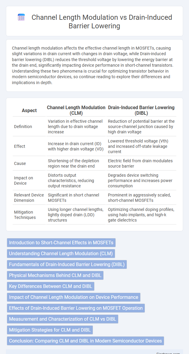
Table of Comparison
| Aspect | Channel Length Modulation (CLM) | Drain-Induced Barrier Lowering (DIBL) |
|---|---|---|
| Definition | Variation in effective channel length due to drain voltage increase | Reduction of potential barrier at the source-channel junction caused by high drain voltage |
| Effect | Increase in drain current (ID) with higher drain voltage (VD) | Lowered threshold voltage (Vth) and increased off-state leakage current |
| Cause | Shortening of the depletion region near the drain end | Electric field from drain modulates source barrier |
| Impact on Device | Distorts output characteristics, reducing output resistance | Degrades device switching performance and increases power consumption |
| Relevant Device Dimension | Significant in short channel MOSFETs | Prominent in aggressively scaled, short-channel MOSFETs |
| Mitigation Techniques | Using longer channel lengths, lightly doped drain (LDD) structures | Optimizing channel doping profiles, using halo implants, and high-k gate dielectrics |
Introduction to Short-Channel Effects in MOSFETs
Short-channel effects in MOSFETs significantly impact device performance as channel lengths shrink below micrometer scales. Channel length modulation occurs when the effective channel length decreases due to increased drain voltage, causing a rise in drain current and reduced output resistance. Drain-induced barrier lowering reduces the potential barrier at the source-channel junction, leading to increased off-state leakage current; understanding these phenomena enables you to optimize transistor behavior in nanoscale integrated circuits.
Understanding Channel Length Modulation (CLM)
Channel Length Modulation (CLM) is a short-channel effect in MOSFETs where the effective channel length decreases as the drain voltage increases, causing an increase in drain current. This phenomenon leads to a non-ideal output characteristic with finite output resistance, impacting analog circuit performance and device linearity. Understanding CLM helps you optimize transistor design by minimizing its effect compared to Drain-Induced Barrier Lowering (DIBL), which primarily reduces the threshold voltage rather than modulating channel length.
Fundamentals of Drain-Induced Barrier Lowering (DIBL)
Drain-Induced Barrier Lowering (DIBL) is a short-channel effect in MOSFET devices where the potential barrier at the source-channel junction is reduced due to increased drain voltage, leading to enhanced carrier injection and increased off-state current. This phenomenon occurs when the depletion region of the drain extends into the channel, effectively lowering the energy barrier and degrading device threshold voltage stability. DIBL critically impacts subthreshold slope, off-state leakage, and overall device scaling, making it a key factor in advanced transistor design and semiconductor manufacturing.
Physical Mechanisms Behind CLM and DIBL
Channel length modulation (CLM) arises from the shortening of the effective channel length in a MOSFET as the drain voltage increases, causing an increase in drain current due to reduced channel resistance. Drain-induced barrier lowering (DIBL) occurs when a high drain voltage lowers the potential barrier at the source-channel junction, facilitating carrier injection and thus decreasing the threshold voltage. Understanding these physical mechanisms helps optimize your transistor design for reduced leakage and improved device performance at nanoscale dimensions.
Key Differences Between CLM and DIBL
Channel length modulation (CLM) and drain-induced barrier lowering (DIBL) both affect MOSFET performance but differ fundamentally in cause and impact; CLM occurs due to the effective shortening of the channel length at high drain voltages, resulting in increased drain current and decreased output resistance. DIBL arises when a high drain voltage lowers the potential barrier at the source-channel junction, reducing the threshold voltage and increasing subthreshold leakage current. Understanding these key differences helps you optimize device design for improved analog or digital circuit performance.
Impact of Channel Length Modulation on Device Performance
Channel length modulation (CLM) significantly affects device performance by causing a reduction in the effective channel length as the drain voltage increases, leading to an increase in drain current and a decrease in output resistance. This phenomenon results in a non-ideal output characteristic and impacts analog circuit gain and switching speed. Understanding CLM's effects is crucial for optimizing transistor design and ensuring your device maintains stable performance across varying operating conditions.
Effects of Drain-Induced Barrier Lowering on MOSFET Operation
Drain-Induced Barrier Lowering (DIBL) significantly impacts MOSFET operation by reducing the threshold voltage as drain voltage increases, causing unwanted leakage currents and degraded device performance. Channel length modulation affects the MOSFET's output characteristics by altering the effective channel length under high drain voltage, but DIBL primarily influences threshold voltage and subthreshold slope. Understanding these effects helps optimize Your transistor design for minimizing short-channel effects and improving switching behavior in advanced CMOS technologies.
Measurement and Characterization of CLM vs DIBL
Measurement of Channel Length Modulation (CLM) typically involves analyzing the change in drain current with varying drain voltage at constant gate voltage, extracting parameters like the channel length modulation coefficient (l) from output characteristic curves. In contrast, Drain-Induced Barrier Lowering (DIBL) is characterized by measuring the threshold voltage shift as a function of drain voltage, often using the transfer characteristics to quantify the effect on subthreshold behavior and short-channel effects. Advanced techniques such as Id-Vg and Id-Vd measurements under varying bias conditions enable accurate extraction of CLM and DIBL parameters critical for compact modeling and device optimization.
Mitigation Strategies for CLM and DIBL
Mitigation strategies for Channel Length Modulation (CLM) include increasing channel doping concentration and optimizing the channel length to reduce variation in effective channel length under high drain bias. For Drain-Induced Barrier Lowering (DIBL), techniques such as using lightly doped drain (LDD) structures, employing high-k gate dielectrics, and enhancing the gate control via multi-gate FET architectures help to minimize drain-induced barrier lowering effects. Advanced device engineering focusing on scaling channel dimensions and improving gate electrostatics significantly suppresses both CLM and DIBL, thus enhancing short-channel device performance and reliability.
Conclusion: Comparing CLM and DIBL in Modern Semiconductor Devices
Channel length modulation (CLM) and drain-induced barrier lowering (DIBL) significantly impact the performance of modern semiconductor devices by affecting current control and threshold voltage stability. CLM primarily causes an increase in drain current due to effective channel shortening at high drain voltages, while DIBL reduces the threshold voltage by lowering the energy barrier at the source-channel junction under high drain bias. In advanced nanoscale transistors, DIBL often poses a greater challenge than CLM due to its stronger influence on leakage currents and device scalability, making DIBL mitigation critical for reliable device operation.
Channel length modulation vs Drain-induced barrier lowering Infographic