GaN HEMTs offer higher electron mobility, faster switching speeds, and greater efficiency compared to Si MOSFETs, making them ideal for high-frequency and high-power applications. Discover which technology best suits your needs by exploring the detailed comparison in the rest of this article.
Table of Comparison
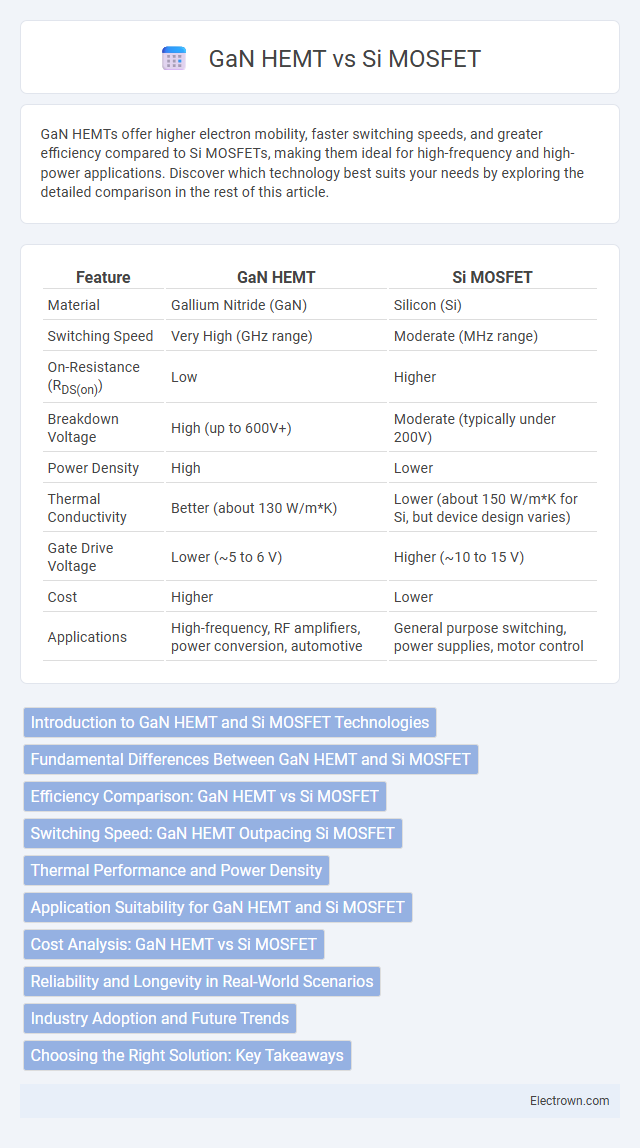
| Feature | GaN HEMT | Si MOSFET |
|---|---|---|
| Material | Gallium Nitride (GaN) | Silicon (Si) |
| Switching Speed | Very High (GHz range) | Moderate (MHz range) |
| On-Resistance (RDS(on)) | Low | Higher |
| Breakdown Voltage | High (up to 600V+) | Moderate (typically under 200V) |
| Power Density | High | Lower |
| Thermal Conductivity | Better (about 130 W/m*K) | Lower (about 150 W/m*K for Si, but device design varies) |
| Gate Drive Voltage | Lower (~5 to 6 V) | Higher (~10 to 15 V) |
| Cost | Higher | Lower |
| Applications | High-frequency, RF amplifiers, power conversion, automotive | General purpose switching, power supplies, motor control |
Introduction to GaN HEMT and Si MOSFET Technologies
GaN HEMT (Gallium Nitride High Electron Mobility Transistor) technology offers superior electron mobility and higher breakdown voltage compared to traditional Si MOSFET (Silicon Metal-Oxide-Semiconductor Field-Effect Transistor) devices, enabling faster switching speeds and improved efficiency. Si MOSFETs, widely used due to their cost-effectiveness and mature manufacturing processes, excel in handling lower power applications with good thermal stability. Your selection between GaN HEMT and Si MOSFET depends on application requirements such as power density, switching frequency, and thermal performance.
Fundamental Differences Between GaN HEMT and Si MOSFET
GaN HEMTs utilize a wide bandgap semiconductor material, gallium nitride, which enables higher electron mobility and greater breakdown voltage compared to silicon-based Si MOSFETs. The heterostructure in GaN HEMTs creates a two-dimensional electron gas (2DEG) channel offering superior electron confinement and ultrafast switching capabilities, whereas Si MOSFETs rely on a silicon oxide gate dielectric and bulk conduction channel. These fundamental differences result in GaN HEMTs delivering higher power density, efficiency, and thermal performance, making them ideal for high-frequency and high-power applications where Si MOSFETs typically face limitations.
Efficiency Comparison: GaN HEMT vs Si MOSFET
GaN HEMTs deliver higher efficiency than Si MOSFETs due to lower on-resistance and faster switching speeds, which reduce conduction and switching losses. The wide bandgap properties of GaN enable operation at higher voltages and frequencies with minimal thermal dissipation, outperforming silicon-based devices in power conversion applications. As a result, GaN HEMTs provide improved energy efficiency and smaller system footprints compared to conventional Si MOSFETs.
Switching Speed: GaN HEMT Outpacing Si MOSFET
GaN HEMT devices achieve significantly higher switching speeds compared to Si MOSFETs due to their superior electron mobility and higher critical electric field, enabling faster charge carrier transport and reduced switching losses. This results in GaN HEMTs operating efficiently at frequencies well into the MHz range, making them ideal for high-frequency power applications such as RF amplifiers and next-generation power converters. Si MOSFETs, constrained by slower switching speeds and higher parasitic capacitances, are generally less effective in these high-speed scenarios.
Thermal Performance and Power Density
GaN HEMTs exhibit superior thermal performance compared to Si MOSFETs due to their wide bandgap properties, allowing operation at higher junction temperatures up to 200degC versus around 150degC for Si MOSFETs. This enhanced thermal capability enables GaN HEMTs to sustain greater power densities, often exceeding 10 W/mm, which is significantly higher than the typical 1-2 W/mm of Si MOSFETs. The combination of high electron mobility and lower on-resistance in GaN HEMTs results in reduced thermal losses and improved efficiency in high-power, high-frequency applications.
Application Suitability for GaN HEMT and Si MOSFET
GaN HEMTs excel in high-frequency, high-power, and high-efficiency applications such as RF amplifiers, 5G base stations, and power converters due to their superior electron mobility and breakdown voltage. Si MOSFETs remain preferable in low to medium power applications, cost-sensitive devices, and general-purpose switching where mature manufacturing and robustness are key factors. Your choice depends on application requirements with GaN HEMTs suited for cutting-edge, high-performance systems while Si MOSFETs cover broad, cost-effective use cases.
Cost Analysis: GaN HEMT vs Si MOSFET
GaN HEMTs generally have higher initial costs compared to Si MOSFETs due to advanced material processing and manufacturing complexities. However, GaN devices offer better efficiency and higher power density, potentially lowering total system costs by reducing cooling and energy expenses. Evaluating your application's performance requirements and volume can reveal whether the upfront investment in GaN HEMTs justifies long-term savings over traditional Si MOSFETs.
Reliability and Longevity in Real-World Scenarios
GaN HEMTs demonstrate superior reliability and longevity in high-frequency and high-temperature environments compared to Si MOSFETs, making them ideal for demanding power electronics applications. Their wide bandgap material enables better thermal stability and reduced electron trapping, leading to enhanced durability under real-world stress conditions. Si MOSFETs, while cost-effective, tend to exhibit increased wear and shorter lifespan when subjected to continuous high voltage and switching cycles.
Industry Adoption and Future Trends
GaN HEMTs are increasingly adopted in high-frequency and high-power applications due to their superior efficiency, faster switching speeds, and higher thermal conductivity compared to Si MOSFETs. The semiconductor industry is shifting towards GaN HEMT technology for power electronics in electric vehicles, 5G infrastructure, and renewable energy systems, driven by demands for miniaturization and energy efficiency. Your choice between GaN HEMT and Si MOSFET will depend on cost considerations and performance requirements, but ongoing advancements suggest GaN's market share will continue to grow rapidly in the next decade.
Choosing the Right Solution: Key Takeaways
GaN HEMTs offer superior switching speeds, higher electron mobility, and greater efficiency compared to Si MOSFETs, making them ideal for high-frequency, high-power applications. Si MOSFETs provide cost-effective solutions with well-established manufacturing processes suited for low to medium power and lower frequency designs. Selecting between GaN HEMT and Si MOSFET hinges on application requirements, balancing factors such as power density, thermal management, switching frequency, and overall system cost.
GaN HEMT vs Si MOSFET Infographic