Nanoscale FETs offer significantly enhanced performance with lower power consumption and higher switching speeds compared to conventional FETs, driven by their reduced channel length and advanced material properties. Explore the detailed comparison to understand how these innovations can impact your electronic device designs.
Table of Comparison
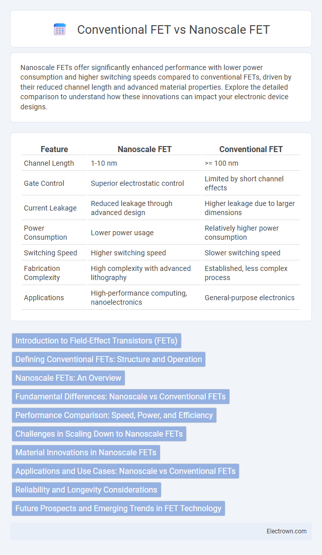
| Feature | Nanoscale FET | Conventional FET |
|---|---|---|
| Channel Length | 1-10 nm | >= 100 nm |
| Gate Control | Superior electrostatic control | Limited by short channel effects |
| Current Leakage | Reduced leakage through advanced design | Higher leakage due to larger dimensions |
| Power Consumption | Lower power usage | Relatively higher power consumption |
| Switching Speed | Higher switching speed | Slower switching speed |
| Fabrication Complexity | High complexity with advanced lithography | Established, less complex process |
| Applications | High-performance computing, nanoelectronics | General-purpose electronics |
Introduction to Field-Effect Transistors (FETs)
Field-Effect Transistors (FETs) control current via an electric field applied to a gate terminal, modulating conductivity in a semiconductor channel. Nanoscale FETs employ channel lengths below 100 nanometers, enhancing device speed and scaling beyond limits of conventional FETs with micrometer-scale channels. The nanoscale design improves gate control, reduces short-channel effects, and supports high-density integration essential for modern integrated circuits.
Defining Conventional FETs: Structure and Operation
Conventional Field-Effect Transistors (FETs) consist of a semiconductor channel controlled by a gate electrode separated by an insulating oxide layer, enabling voltage modulation of current flow between the source and drain terminals. Their operation relies on forming a conductive channel in a bulk semiconductor material, with electron mobility and channel length dictating switching speed and power consumption. Understanding Your device's performance begins with recognizing how these traditional planar structures contrast with the reduced dimensions and electrical behaviors of nanoscale FETs.
Nanoscale FETs: An Overview
Nanoscale Field-Effect Transistors (FETs) exhibit superior electrical performance compared to conventional FETs due to their reduced channel length, enabling faster switching speeds and lower power consumption. Quantum effects and short-channel phenomena become significant in nanoscale FETs, requiring advanced materials like high-k dielectrics and novel device structures to maintain scalability and reliability. Your integration of nanoscale FETs in modern electronics improves device density and enhances overall system efficiency, making them crucial for next-generation semiconductor technology.
Fundamental Differences: Nanoscale vs Conventional FETs
Nanoscale FETs operate at atomic or molecular dimensions, allowing for enhanced control over electron transport compared to conventional FETs, which function at larger scales with less precision. The fundamental difference lies in quantum effects and short-channel phenomena dominating nanoscale FET behavior, resulting in increased speed and lower power consumption. Your device performance can benefit significantly from the superior electrostatic control and reduced leakage currents characteristic of nanoscale FETs.
Performance Comparison: Speed, Power, and Efficiency
Nanoscale FETs demonstrate significantly higher speed and switching performance than conventional FETs due to reduced channel lengths and enhanced electron mobility at the nanoscale. Your device's power consumption benefits from the lower operating voltage and leakage currents, resulting in improved energy efficiency compared to traditional FETs. These factors collectively make nanoscale FETs a superior choice for high-performance, low-power applications in modern electronics.
Challenges in Scaling Down to Nanoscale FETs
Scaling down to nanoscale FETs introduces significant challenges such as short-channel effects, increased leakage currents, and variability in device performance due to quantum mechanical phenomena. Precise control over channel length and doping profiles is critical to maintaining device reliability and minimizing power consumption in nanoscale regimes. Advanced materials and innovative fabrication techniques are essential to overcome limitations posed by conventional lithography and to ensure stable operation of nanoscale FETs.
Material Innovations in Nanoscale FETs
Nanoscale FETs leverage advanced materials such as graphene, transition metal dichalcogenides (TMDs), and silicon nanowires to achieve superior electrical performance and scaling beyond conventional silicon-based FETs. These materials offer higher electron mobility, reduced short-channel effects, and enhanced gate control, enabling lower power consumption and faster switching speeds. Innovations in high-k dielectrics and 2D material heterostructures further optimize device scalability and stability in nanoscale FET architectures.
Applications and Use Cases: Nanoscale vs Conventional FETs
Nanoscale FETs enable advanced applications in high-density integrated circuits, quantum computing, and ultra-low power electronics due to their superior electron mobility and reduced short-channel effects. Conventional FETs remain prevalent in everyday consumer electronics, power amplifiers, and analog circuits where cost-efficiency and established fabrication processes are critical. The shift towards nanoscale FETs supports next-generation technologies requiring smaller footprints, higher speeds, and greater energy efficiency compared to traditional FETs.
Reliability and Longevity Considerations
Nanoscale FETs exhibit enhanced reliability challenges due to increased susceptibility to short-channel effects, gate leakage, and variability in nanoscale dimensions compared to conventional FETs. Advanced materials and precise fabrication techniques improve the longevity of nanoscale FETs by mitigating degradation mechanisms such as hot carrier injection and bias temperature instability. Despite these advances, conventional FETs generally offer superior long-term stability in less aggressive scaling environments.
Future Prospects and Emerging Trends in FET Technology
Nanoscale FETs offer unprecedented scaling potential, enabling higher device density and faster switching speeds compared to conventional FETs constrained by short-channel effects and power dissipation issues. Emerging trends emphasize incorporating novel materials like 2D semiconductors and graphene to enhance carrier mobility and reduce leakage currents, which are challenges for silicon-based FETs. The future prospects highlight integrating nanoscale FETs in low-power, high-performance applications including AI processors and flexible electronics, driving innovation in semiconductor device architecture.
Nanoscale FET vs conventional FET Infographic