Deep N-well and Triple-well technologies enhance isolation and reduce substrate noise in CMOS circuits, with Deep N-well providing a single deep isolation layer, while Triple-well includes an additional well for improved electrical characteristics and latch-up immunity. Explore the rest of the article to understand how each structure impacts your circuit design and performance.
Table of Comparison
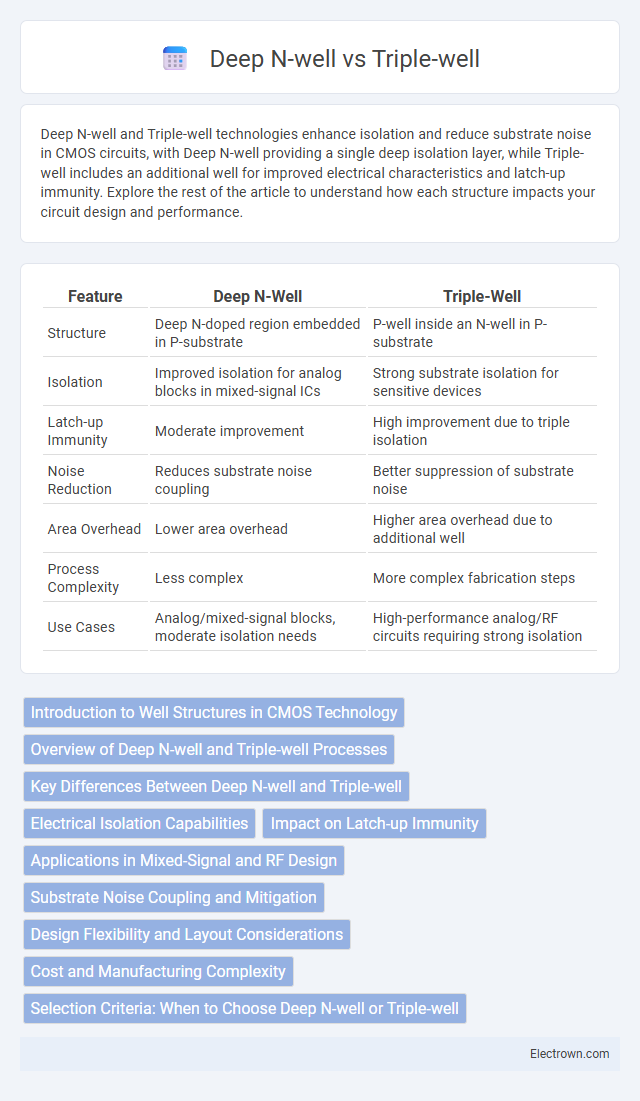
| Feature | Deep N-Well | Triple-Well |
|---|---|---|
| Structure | Deep N-doped region embedded in P-substrate | P-well inside an N-well in P-substrate |
| Isolation | Improved isolation for analog blocks in mixed-signal ICs | Strong substrate isolation for sensitive devices |
| Latch-up Immunity | Moderate improvement | High improvement due to triple isolation |
| Noise Reduction | Reduces substrate noise coupling | Better suppression of substrate noise |
| Area Overhead | Lower area overhead | Higher area overhead due to additional well |
| Process Complexity | Less complex | More complex fabrication steps |
| Use Cases | Analog/mixed-signal blocks, moderate isolation needs | High-performance analog/RF circuits requiring strong isolation |
Introduction to Well Structures in CMOS Technology
Deep N-well and Triple-well structures in CMOS technology enhance device isolation and latch-up immunity by incorporating multiple well regions within the semiconductor substrate. Deep N-well allows for the integration of PMOS transistors in an isolated N-well beneath the P-substrate, improving noise immunity and reducing substrate coupling. Triple-well adds an extra P-well inside the deep N-well, providing superior isolation for both NMOS and PMOS devices, which is crucial for mixed-signal and high-voltage applications in your integrated circuits.
Overview of Deep N-well and Triple-well Processes
Deep N-well and Triple-well processes enhance isolation in CMOS fabrication by creating additional wells within the substrate, improving latch-up immunity and device performance. The Deep N-well process involves a thick, heavily doped N-type region beneath the standard P-well, offering superior isolation for analog and mixed-signal circuits. Triple-well technology adds both a Deep N-well and a P-well inside it, allowing more precise control of body biasing and reducing substrate noise, which optimizes your integrated circuit performance.
Key Differences Between Deep N-well and Triple-well
Deep N-well technology involves embedding a large N-well region within a P-substrate to isolate PMOS transistors and reduce substrate noise, improving latch-up immunity and analog performance. Triple-well integrates a deep N-well enclosing a P-well inside the substrate, enabling independent biasing of NMOS transistors and enhanced noise isolation between analog and digital blocks. The key difference lies in the triple-well's additional P-well layer providing better isolation and bias control compared to the single deep N-well, benefiting mixed-signal IC designs.
Electrical Isolation Capabilities
Deep N-well technology offers enhanced electrical isolation by creating a robust barrier that minimizes substrate noise coupling and latch-up risk, making it suitable for mixed-signal and high-voltage applications. Triple-well structures provide separate wells for NMOS and PMOS transistors, allowing independent biasing and improved isolation between circuit blocks but may not suppress substrate noise as effectively as deep N-wells. Choosing the appropriate isolation technique depends on your circuit's sensitivity to noise and the required level of latch-up immunity.
Impact on Latch-up Immunity
Deep N-well technology significantly enhances latch-up immunity by providing a robust isolation barrier that prevents parasitic thyristor formation and reduces substrate coupling. Triple-well processes improve latch-up resilience by enabling individual well biasing for NMOS and PMOS transistors, minimizing well-to-substrate leakage and suppressing latch-up triggering. Compared to triple-well, deep N-well offers superior latch-up suppression in mixed-signal and high-voltage applications due to its deeper isolation and enhanced substrate noise immunity.
Applications in Mixed-Signal and RF Design
Deep N-well and triple-well technologies enhance isolation in mixed-signal and RF design by reducing substrate noise coupling and latch-up susceptibility, critical for maintaining signal integrity. Deep N-well structures provide a dedicated well for analog or sensitive circuits, minimizing interference from digital switching activities. Triple-well processes offer even greater isolation by enabling independent biasing of wells, optimizing performance in integrated transceivers and high-frequency analog components.
Substrate Noise Coupling and Mitigation
Deep N-well (DNW) and Triple-well structures play critical roles in substrate noise coupling mitigation in mixed-signal ICs. DNW reduces substrate noise by creating a low-resistance isolation region around sensitive analog devices, effectively blocking noise propagation from digital circuitry. Triple-well offers enhanced isolation by embedding an additional well layer, allowing independent biasing that further suppresses substrate noise coupling and improves overall analog performance in high-density integrations.
Design Flexibility and Layout Considerations
Deep N-well technology enhances design flexibility by enabling independent biasing of N-well regions, allowing better isolation of sensitive analog circuits from noisy digital blocks. Triple-well structures provide similar isolation but with more complex layout constraints due to the additional P-well layer, which can impact cell placement and routing density. Layout considerations for deep N-well favor simplified substrate noise management and reduced latch-up risk, whereas triple-well offers finer control over well potentials at the cost of increased area and higher process complexity.
Cost and Manufacturing Complexity
Deep N-well technology involves additional ion implantation steps leading to increased manufacturing complexity and moderate cost increments compared to standard processes. Triple-well structures require multiple well isolations and higher lithography precision, contributing to higher fabrication costs and more complex process control. The choice between Deep N-well and Triple-well often balances device performance requirements against the available budget and fabrication capabilities in semiconductor manufacturing.
Selection Criteria: When to Choose Deep N-well or Triple-well
Deep N-well technology is ideal for isolating sensitive analog circuits from noisy digital substrates in mixed-signal ICs, offering improved noise immunity and latch-up prevention. Triple-well structures provide enhanced substrate isolation suitable for high-voltage applications and RF circuits where deep isolation and independent well biasing are crucial. Selection between Deep N-well and Triple-well depends on the specific noise isolation requirements, biasing flexibility, and voltage levels of the target application.
Deep N-well vs Triple-well Infographic