Planarization and etch back are critical semiconductor fabrication techniques used to achieve uniform surface topography, with planarization focusing on polishing layers to create a flat surface and etch back removing excess material through selective etching. Understanding the differences between these methods can greatly enhance your fabrication process control; explore the rest of the article to learn which technique suits your specific application needs.
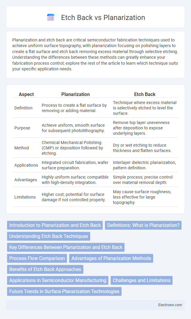
Table of Comparison
| Aspect | Planarization | Etch Back |
|---|---|---|
| Definition | Process to create a flat surface by removing or adding material. | Technique where excess material is selectively etched to level the surface. |
| Purpose | Achieve uniform, smooth surface for subsequent photolithography. | Remove top layer unevenness after deposition to expose underlying layers. |
| Method | Chemical Mechanical Polishing (CMP) or deposition followed by etching. | Dry or wet etching to reduce thickness and flatten surfaces. |
| Applications | Integrated circuit fabrication, wafer surface preparation. | Interlayer dielectric planarization, pattern definition. |
| Advantages | Highly uniform surface; compatible with high-density integration. | Simple process; precise control over material removal depth. |
| Limitations | Higher cost; potential for surface damage if not controlled properly. | May cause surface roughness; less effective for large topography. |
Introduction to Planarization and Etch Back
Planarization and etch back are critical processes in semiconductor manufacturing used to achieve a flat surface for subsequent photolithography steps. Planarization typically employs chemical mechanical polishing (CMP) to smooth and level layers, ensuring uniform thickness across the wafer. Etch back involves selective removal of excess material through controlled etching, allowing precise surface profile adjustments tailored to your device architecture.
Definitions: What is Planarization?
Planarization is a semiconductor fabrication process that smooths and flattens the surface of a wafer to create a uniform topology, essential for subsequent photolithography steps. It commonly utilizes chemical mechanical polishing (CMP) to remove excess material and achieve a level surface. This technique enhances layer uniformity and device performance by minimizing surface irregularities and thickness variations.
Understanding Etch Back Techniques
Etch back techniques in planarization involve selectively removing excess material from the wafer surface to achieve a uniform layer without damaging underlying structures. This method precisely targets dielectric or photoresist layers, optimizing surface flatness critical for subsequent lithography steps. Understanding etch back parameters such as etch rate, uniformity, and selectivity enhances process control versus traditional chemical-mechanical polishing (CMP) methods.
Key Differences Between Planarization and Etch Back
Planarization creates a smooth, even surface on semiconductor wafers by depositing and polishing layers, while etch back removes excess material using controlled etching processes to achieve surface uniformity. Planarization often involves chemical mechanical polishing (CMP) for precision, whereas etch back relies on selective etching, impacting layer thickness control differently. Understanding these key differences helps optimize your fabrication process for improved device performance and reliability.
Process Flow Comparison
Planarization involves deposition of a dielectric film followed by chemical mechanical polishing (CMP) to achieve a flat surface, while etch back relies on uniform dielectric deposition and anisotropic etching to remove excess material. The planarization process flow typically includes film deposition, polishing, cleaning, and inspection, ensuring global uniformity and minimal topography variation. Etch back requires careful control during etching to prevent surface roughness and non-uniformity, often involving plasma etching steps after deposition without the polishing phase present in planarization.
Advantages of Planarization Methods
Planarization methods offer superior surface uniformity compared to etch back, enhancing the reliability and performance of semiconductor devices by reducing topographical variations. These techniques, such as chemical mechanical polishing (CMP), provide better control over film thickness and improve subsequent photolithography steps. Your manufacturing process benefits from increased yield and device consistency when implementing planarization.
Benefits of Etch Back Approaches
Etch back techniques offer precise control over surface topography, enabling uniform layer thickness and improved planar surfaces essential for high-resolution semiconductor fabrication. This method reduces defects and enhances device performance by minimizing dishing and erosion compared to traditional planarization methods. Your processes benefit from increased consistency and compatibility with delicate materials in advanced microelectronics manufacturing.
Applications in Semiconductor Manufacturing
Planarization and etch back techniques are essential in semiconductor manufacturing for achieving uniform surface topographies, critical for multilayer photolithography and device performance. Planarization methods, such as chemical mechanical polishing (CMP), are widely applied to create smooth surfaces on interlayer dielectrics and metal layers, improving circuit pattern fidelity. Etch back processes selectively remove excess material, often utilized in defining shallow trench isolation and polishing photoresist layers, ensuring precise feature dimensions and electrical isolation in integrated circuits.
Challenges and Limitations
Planarization techniques like chemical mechanical polishing (CMP) face challenges such as non-uniform material removal and substrate damage, affecting wafer surface flatness. Etch back processes contend with limitations including difficult endpoint control and potential over-etching, which can degrade critical dimensions and device performance. Your choice between these methods depends on trade-offs in precision, throughput, and compatibility with subsequent fabrication steps.
Future Trends in Surface Planarization Technologies
Future trends in surface planarization technologies emphasize the integration of chemical mechanical planarization (CMP) with advanced etch back techniques to achieve ultra-flat surfaces at the nanoscale. Emerging methods leverage precision control and real-time monitoring to optimize material removal rates, minimizing defects and enhancing device performance. Your semiconductor manufacturing processes will benefit from these innovations, enabling higher density and reliability in next-generation microelectronics.
Planarization vs etch back Infographic