P-well and N-well processes are key techniques in CMOS fabrication, each designed to house NMOS and PMOS transistors respectively, ensuring optimal electrical isolation and performance. Understanding how these well types influence device characteristics can help you choose the right process for your semiconductor design projects; continue reading to explore their differences and applications in detail.
Table of Comparison
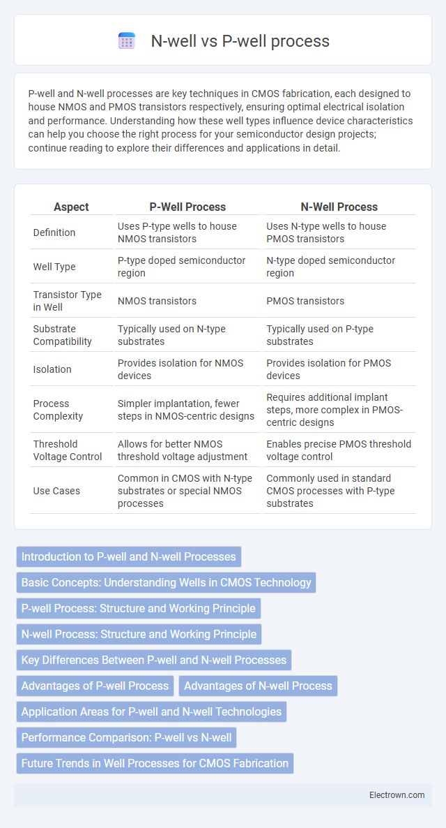
| Aspect | P-Well Process | N-Well Process |
|---|---|---|
| Definition | Uses P-type wells to house NMOS transistors | Uses N-type wells to house PMOS transistors |
| Well Type | P-type doped semiconductor region | N-type doped semiconductor region |
| Transistor Type in Well | NMOS transistors | PMOS transistors |
| Substrate Compatibility | Typically used on N-type substrates | Typically used on P-type substrates |
| Isolation | Provides isolation for NMOS devices | Provides isolation for PMOS devices |
| Process Complexity | Simpler implantation, fewer steps in NMOS-centric designs | Requires additional implant steps, more complex in PMOS-centric designs |
| Threshold Voltage Control | Allows for better NMOS threshold voltage adjustment | Enables precise PMOS threshold voltage control |
| Use Cases | Common in CMOS with N-type substrates or special NMOS processes | Commonly used in standard CMOS processes with P-type substrates |
Introduction to P-well and N-well Processes
P-well and N-well processes are fundamental techniques in CMOS (Complementary Metal-Oxide-Semiconductor) technology used to create p-type and n-type regions respectively within a silicon substrate. The P-well process forms a p-type well in an n-type substrate, enabling the integration of NMOS transistors, while the N-well process creates an n-type well in a p-type substrate for PMOS transistor fabrication. These well regions are essential for isolating transistor types, enabling complementary operation and enhancing device performance in integrated circuits.
Basic Concepts: Understanding Wells in CMOS Technology
P-well and N-well processes are fundamental techniques in CMOS technology used to create complementary transistors on a single silicon substrate. In the P-well process, a p-type region is implanted into an n-type substrate to form the body for NMOS transistors, while the N-well process involves implanting an n-type region into a p-type substrate to house PMOS transistors. Your choice between these well structures affects transistor threshold voltages, latch-up susceptibility, and overall device performance.
P-well Process: Structure and Working Principle
The P-well process involves creating a p-type region within an n-type substrate, serving as the foundation for n-channel MOSFETs in CMOS technology. This structure allows for the isolation of p-type transistors in integrated circuits, enabling complementary device integration with N-well regions for p-channel MOSFETs. The working principle relies on controlling charge carriers by biasing the p-well to prevent latch-up and optimize circuit performance through precise doping concentrations and well dimensions.
N-well Process: Structure and Working Principle
The N-well process involves creating a positively doped region within a negatively doped p-type silicon substrate to form isolated n-type areas, crucial for integrating PMOS transistors in CMOS technology. This process enables the formation of well-defined junctions by implanting or diffusing donor impurities such as phosphorus or arsenic, which modulate electrical characteristics like threshold voltage and leakage currents. The N-well serves as the body or bulk region for PMOS devices, providing isolation and allowing independent biasing to optimize transistor performance and reduce parasitic effects.
Key Differences Between P-well and N-well Processes
P-well and N-well processes differ primarily in the type of substrate doping and well formation used in CMOS fabrication, where P-well processes involve creating p-type wells in an n-type substrate, while N-well processes form n-type wells in a p-type substrate. The P-well process enhances NMOS transistor performance by isolating the p-type regions, whereas the N-well process optimizes PMOS device characteristics by embedding n-type wells. These foundational differences impact the electrical properties, device isolation, and compatibility with specific CMOS technologies, influencing overall circuit integration and performance.
Advantages of P-well Process
The P-well process offers improved integration for NMOS transistors by providing a low-resistance substrate that enhances electron mobility and reduces latch-up susceptibility in CMOS circuits. It enables precise control over threshold voltage, leading to better device performance and power efficiency. Additionally, the P-well process facilitates higher packing density and improved isolation between devices, essential for advanced semiconductor fabrication.
Advantages of N-well Process
N-well process offers improved isolation for PMOS transistors by implanting a lightly doped N-type region in a P-type substrate, reducing latch-up susceptibility in CMOS circuits. This process enables higher noise immunity and better threshold voltage control for NMOS devices, enhancing overall circuit performance. Your designs benefit from increased integration density and more robust device characteristics with the N-well approach.
Application Areas for P-well and N-well Technologies
P-well technology is primarily used in NMOS transistor fabrication, making it ideal for digital circuits and high-speed logic applications due to its lower electron mobility and leakage current. N-well technology supports PMOS transistor creation, which is essential for complementary metal-oxide-semiconductor (CMOS) devices, enabling efficient power management and analog circuit design. Your choice between P-well and N-well processes directly impacts the performance and power consumption of integrated circuits in applications ranging from microprocessors to sensor interfaces.
Performance Comparison: P-well vs N-well
The P-well process offers enhanced electron mobility compared to the N-well process, leading to faster NMOS transistor switching speeds and improved overall circuit performance. N-well processes provide superior hole mobility, which benefits PMOS devices but may result in slower NMOS transistors relative to P-well designs. Performance optimization depends on the specific application requirements, with P-well favoring high-speed NMOS functionality and N-well enabling balanced CMOS integration.
Future Trends in Well Processes for CMOS Fabrication
Future trends in well processes for CMOS fabrication emphasize advanced doping techniques and scalable well designs to enhance device performance and reduce leakage currents. Innovations such as fin-based P-well and N-well structures improve electrostatic control and support ultra-thin body transistors in sub-3nm nodes. You can expect increased integration of 3D well architectures and selective epitaxy to optimize carrier mobility and enable heterogeneous integration for next-generation semiconductor devices.
P-well vs N-well process Infographic