Thin-film technology offers higher precision and better performance in electronic components due to its uniform layer deposition, while thick-film technology is more cost-effective and suitable for mass production with robust mechanical properties. Explore the full article to discover how your choice between thin-film and thick-film technology impacts your project's efficiency and cost.
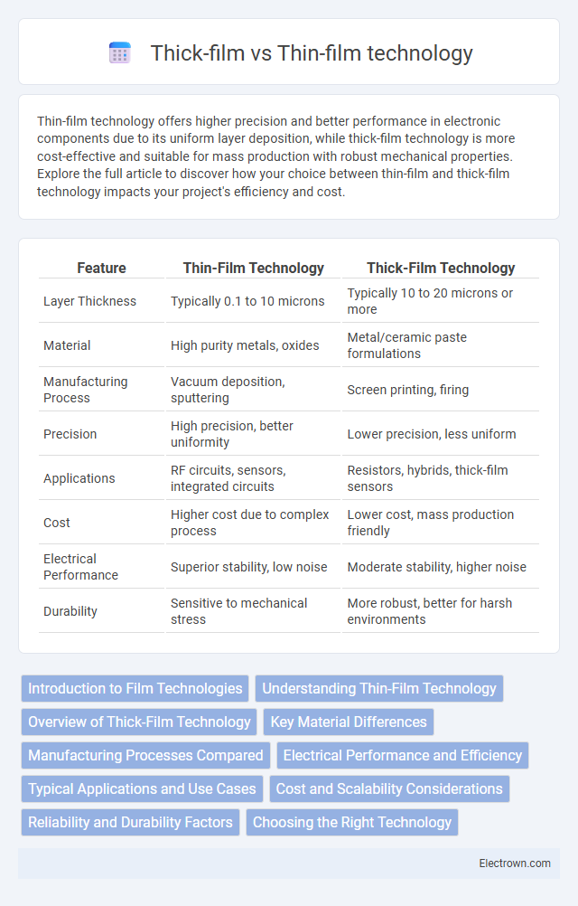
Table of Comparison
| Feature | Thin-Film Technology | Thick-Film Technology |
|---|---|---|
| Layer Thickness | Typically 0.1 to 10 microns | Typically 10 to 20 microns or more |
| Material | High purity metals, oxides | Metal/ceramic paste formulations |
| Manufacturing Process | Vacuum deposition, sputtering | Screen printing, firing |
| Precision | High precision, better uniformity | Lower precision, less uniform |
| Applications | RF circuits, sensors, integrated circuits | Resistors, hybrids, thick-film sensors |
| Cost | Higher cost due to complex process | Lower cost, mass production friendly |
| Electrical Performance | Superior stability, low noise | Moderate stability, higher noise |
| Durability | Sensitive to mechanical stress | More robust, better for harsh environments |
Introduction to Film Technologies
Thin-film and thick-film technologies refer to distinct methods of depositing electronic circuits onto substrates, with thin-film involving precise vapor deposition of materials at micrometer thicknesses, while thick-film utilizes screen-printing of paste-based materials followed by firing. Thin-film technology offers higher precision, better electrical performance, and is commonly used in applications like RF circuits and sensors, whereas thick-film technology is valued for its cost-effectiveness and durability in power hybrid circuits and resistors. Both technologies are fundamental in manufacturing multilayer electronic components but differ significantly in process complexity, material composition, and typical application domains.
Understanding Thin-Film Technology
Thin-film technology involves depositing ultra-thin layers of conductive or resistive materials onto insulating substrates using methods such as sputtering or evaporation. This process enables precise control over electrical properties and film thickness, resulting in high performance and reliability in applications like sensors, circuit components, and microelectronics. Your designs can benefit from thin-film technology's superior accuracy, thermal stability, and miniaturization potential compared to thick-film alternatives.
Overview of Thick-Film Technology
Thick-film technology involves the deposition of multiple layers of conductive, resistive, and dielectric pastes onto ceramic substrates, followed by firing at high temperatures to form durable, precise circuits. Commonly used in hybrid microelectronics, thick-film circuits provide excellent mechanical strength, high power handling, and compatibility with various substrates. This technology is ideal for manufacturing resistors, capacitors, and integrated circuits in automotive, aerospace, and industrial applications due to its cost-effectiveness and versatility.
Key Material Differences
Thin-film technology uses materials like sputtered metals or metal oxides deposited in extremely thin layers, typically under 10 microns, offering precise electrical characteristics and superior performance at high frequencies. Thick-film technology relies on printable pastes composed of conductive, resistive, or dielectric materials deposited in thicker layers, generally between 10-100 microns, which provide cost-effective manufacturing and robustness. Your choice between thin-film and thick-film depends on the required precision, frequency response, and budget constraints tied to these material distinctions.
Manufacturing Processes Compared
Thin-film technology employs vacuum deposition techniques such as sputtering or chemical vapor deposition to create ultra-thin layers of conductive or resistive materials on ceramic or glass substrates, resulting in high precision and performance components. Thick-film technology uses screen printing or stencil printing to apply paste-based materials onto substrates, followed by firing at high temperatures, which allows for cost-effective production of durable components with thicker, more robust layers. Your choice between these manufacturing processes depends on factors like desired electrical characteristics, production volume, and cost constraints.
Electrical Performance and Efficiency
Thin-film technology offers superior electrical performance with lower resistance, higher precision, and better frequency response compared to thick-film technology, which typically exhibits higher parasitic losses and less uniformity. Thin films provide enhanced efficiency in high-frequency applications due to their reduced thickness and improved material properties, resulting in minimal signal attenuation and greater stability. Thick-film technology, while more cost-effective for high-power and robust applications, often sacrifices some electrical performance and efficiency owing to its comparatively rougher texture and thicker conductive layers.
Typical Applications and Use Cases
Thin-film technology excels in high-precision applications such as aerospace instrumentation, medical devices, and RF circuits due to its superior accuracy and stability. Thick-film technology is widely used in power electronics, automotive sensors, and industrial controls where cost-effectiveness and durability under harsh conditions are crucial. Your choice depends on the specific performance requirements and environmental conditions of your application.
Cost and Scalability Considerations
Thin-film technology offers higher precision and better performance at a generally higher cost, making it suitable for applications requiring fine detail and electrical stability. Thick-film technology provides a more cost-effective solution with simpler manufacturing processes, which supports larger volume production and better scalability for mass-market products. Cost efficiency in thick-film manufacturing results from using printable pastes and standard substrates, while thin-film's scalability is constrained by more complex fabrication techniques and equipment.
Reliability and Durability Factors
Thin-film technology offers superior reliability and durability due to its precise deposition process, which results in higher resistance to thermal stress and mechanical wear compared to thick-film technology. The dense and uniform layers in thin-film components minimize the risk of cracks and delamination, enhancing long-term stability in harsh environments. Thick-film technology, while cost-effective, is more prone to micro-cracking and variations in layer adhesion, potentially reducing lifespan under repeated thermal cycling and mechanical strain.
Choosing the Right Technology
Selecting the appropriate technology between thin-film and thick-film depends on the application's precision, size constraints, and cost considerations. Thin-film technology offers superior accuracy and stability, making it ideal for high-frequency and sensitive circuits, while thick-film is cost-effective and robust for power electronics and large-volume production. Evaluating the specific electrical performance requirements and environmental conditions ensures the optimal choice between these two film deposition methods.
Thin-film vs thick-film technology Infographic