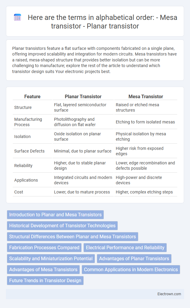
Planar transistors feature a flat surface with components fabricated on a single plane, offering improved scalability and integration for modern circuits. Mesa transistors have a raised, mesa-shaped structure that provides better isolation but can be more challenging to manufacture; explore the rest of the article to understand which transistor design suits Your electronic projects best.
Table of Comparison
| Feature | Planar Transistor | Mesa Transistor |
|---|---|---|
| Structure | Flat, layered semiconductor surface | Raised or etched mesa structures |
| Manufacturing Process | Photolithography and diffusion on flat wafer | Etching to form isolated mesas |
| Isolation | Oxide isolation on planar surface | Physical isolation by mesa etching |
| Surface Defects | Minimal, due to planar surface | Higher risk from exposed edges |
| Reliability | Higher, due to stable planar design | Lower, edge recombination and defects possible |
| Applications | Integrated circuits and modern devices | High-power and discrete devices |
| Cost | Lower, due to mature process | Higher, complex etching steps |
Introduction to Planar and Mesa Transistors
Planar transistors feature a flat semiconductor surface with junctions fabricated through diffusion and oxidation processes, enabling enhanced scalability and integration. Mesa transistors have a raised, etched structure with exposed junction edges, offering robust performance but increased surface leakage and complexity. The planar design dominates modern semiconductor manufacturing due to superior reliability and ease of mass production.
Historical Development of Transistor Technologies
The historical development of transistor technologies highlights the transition from mesa transistors, which were among the first practical semiconductor devices, to planar transistors that revolutionized manufacturing with improved surface passivation and scalability. Mesa transistors, developed in the early 1950s, featured exposed junctions susceptible to contamination, limiting reliability and integration density. Planar technology, introduced by Jean Hoerni in 1959, enabled the production of more durable and compact transistors essential for modern integrated circuits, significantly advancing semiconductor device performance and enabling your electronic devices' miniaturization.
Structural Differences Between Planar and Mesa Transistors
Planar transistors feature a flat surface with junctions formed beneath an oxide layer, allowing for better integration and reduced surface defects. Mesa transistors have a raised, etched structure exposing the active region, which can lead to higher surface recombination and increased leakage currents. Understanding these structural differences helps you choose the right transistor type for improved device performance and reliability.
Fabrication Processes Compared
Planar transistors are fabricated using photolithography to create flat, closely packed semiconductor layers on a silicon wafer, offering superior integration density and easier doping control. Mesa transistors involve etching away surrounding material to form a raised "mesa" structure, which can enhance device isolation but increases fabrication complexity and cost. Your choice depends on the application, with planar transistors favored for large-scale integrated circuits and mesa transistors utilized in high-power or specialized optoelectronic devices.
Electrical Performance and Reliability
Planar transistors exhibit superior electrical performance due to their lower parasitic capacitance and higher switching speeds compared to mesa transistors. Mesa transistors often face reliability challenges stemming from surface recombination and leakage currents caused by their exposed sidewalls. Optimizing your circuit's performance and longevity favors planar transistor technology for improved stability and efficiency.
Scalability and Miniaturization Potential
Planar transistors offer superior scalability due to their flat surface design, enabling easier photolithographic patterning and higher transistor density on silicon wafers. Mesa transistors, with their raised mesa structures, face physical limitations in miniaturization since the etched sidewalls complicate scaling down device dimensions without increasing surface defects. Consequently, planar transistors dominate modern integrated circuit fabrication, supporting continued device miniaturization and enhanced performance in advanced semiconductor technologies.
Advantages of Planar Transistors
Planar transistors offer superior miniaturization and reliability due to their flat, surface-level design, enabling higher integration density in integrated circuits. They provide enhanced electrical performance with lower parasitic capacitance and improved thermal stability compared to mesa transistors. Manufacturing planar transistors is more cost-effective and scalable, driven by established photolithographic processes that reduce defects and increase yield.
Advantages of Mesa Transistors
Mesa transistors offer enhanced isolation between devices due to their raised structure, which reduces parasitic capacitance and leakage currents. The distinct mesa etching allows for better control of the active region, improving device reliability and breakdown voltage. This architecture also facilitates easier heat dissipation, resulting in improved thermal stability compared to planar transistors.
Common Applications in Modern Electronics
Planar transistors are widely used in integrated circuits for consumer electronics, such as smartphones and computers, due to their compact design and ease of mass production. Mesa transistors find common applications in high-power and high-frequency devices, including RF amplifiers and microwave communication systems, where superior thermal stability and performance are critical. Your choice between planar and mesa transistors depends on the specific electronic application's power and frequency requirements.
Future Trends in Transistor Design
Emerging transistor designs increasingly favor planar structures due to their superior scalability and reduced short-channel effects compared to traditional mesa transistors. Advances in semiconductor fabrication techniques, such as extreme ultraviolet (EUV) lithography, enable improved planar transistor miniaturization, fostering higher performance and energy efficiency in integrated circuits. Research into novel materials like silicon carbide and gallium nitride further supports planar transistor evolution, positioning them at the forefront of next-generation electronics and high-frequency applications.
planar transistor vs mesa transistor Infographic