A 4-layer PCB offers enhanced signal integrity, better electromagnetic interference (EMI) shielding, and improved power distribution compared to a 2-layer PCB, making it ideal for complex and high-performance electronic designs. Explore the rest of the article to understand which PCB type best suits your project needs.
Table of Comparison
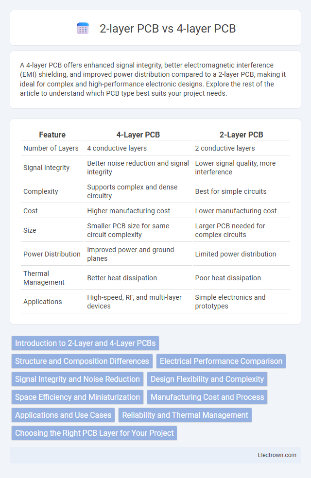
| Feature | 4-Layer PCB | 2-Layer PCB |
|---|---|---|
| Number of Layers | 4 conductive layers | 2 conductive layers |
| Signal Integrity | Better noise reduction and signal integrity | Lower signal quality, more interference |
| Complexity | Supports complex and dense circuitry | Best for simple circuits |
| Cost | Higher manufacturing cost | Lower manufacturing cost |
| Size | Smaller PCB size for same circuit complexity | Larger PCB needed for complex circuits |
| Power Distribution | Improved power and ground planes | Limited power distribution |
| Thermal Management | Better heat dissipation | Poor heat dissipation |
| Applications | High-speed, RF, and multi-layer devices | Simple electronics and prototypes |
Introduction to 2-Layer and 4-Layer PCBs
2-layer PCBs consist of two conductive copper layers separated by a dielectric substrate, offering simple routing for basic electronic circuits. 4-layer PCBs incorporate four copper layers, including dedicated power and ground planes, enhancing signal integrity and reducing electromagnetic interference. Choosing your PCB depends on circuit complexity, with 4-layer designs providing better performance for high-speed or densely packed components.
Structure and Composition Differences
A 4-layer PCB consists of four layers of conductive copper separated by insulating materials, typically including two signal layers and two power or ground planes, enhancing signal integrity and electromagnetic interference reduction. In contrast, a 2-layer PCB has only two copper layers, usually one for signals and one for ground or power, limiting its complexity and electromagnetic shielding capabilities. Your choice between a 4-layer and 2-layer PCB depends on the need for multi-layer routing, improved electrical performance, and compact design requirements.
Electrical Performance Comparison
Four-layer PCBs offer superior electrical performance compared to two-layer PCBs due to their additional internal layers, which enable better signal integrity, reduced electromagnetic interference (EMI), and improved power distribution. The dedicated ground and power planes in a 4-layer PCB minimize noise and crosstalk, enhancing overall circuit stability and high-frequency handling. Your design benefits from lower inductance and impedance control, critical for complex and high-speed electronic applications.
Signal Integrity and Noise Reduction
A 4-layer PCB significantly enhances signal integrity and noise reduction compared to a 2-layer PCB by providing dedicated ground and power planes that minimize electromagnetic interference and crosstalk. The additional layers enable better impedance control and shielding, resulting in cleaner signal transmission and reduced signal degradation. For your high-frequency or sensitive circuit designs, a 4-layer PCB offers superior performance and reliability in maintaining signal quality.
Design Flexibility and Complexity
4-layer PCBs offer significantly greater design flexibility compared to 2-layer PCBs, allowing for advanced signal integrity, reduced electromagnetic interference, and improved power distribution due to dedicated ground and power planes. The increased complexity of 4-layer PCB layouts enables more compact component placement and supports higher-density circuitry essential for modern electronics. Your choice hinges on balancing the need for sophisticated design capabilities with cost and manufacturing considerations.
Space Efficiency and Miniaturization
A 4-layer PCB offers greater space efficiency and supports miniaturization by providing additional routing layers, which allows complex circuits to be designed on a smaller footprint compared to a 2-layer PCB. Your device can benefit from enhanced signal integrity and reduced electromagnetic interference due to dedicated ground and power planes in 4-layer boards. This extra flexibility enables more compact and efficient electronic designs, ideal for modern, high-performance applications.
Manufacturing Cost and Process
A 4-layer PCB typically involves higher manufacturing costs than a 2-layer PCB due to additional material layers, more complex lamination processes, and increased drilling requirements. The manufacturing process of a 4-layer PCB requires precise alignment and insulation between internal layers, extending fabrication time and resource consumption. In contrast, 2-layer PCBs feature simpler production steps, lower material usage, and reduced drilling complexity, resulting in cost-effective manufacturing suited for basic electronic designs.
Applications and Use Cases
4-layer PCBs are ideal for complex applications like high-speed communication devices, advanced computing hardware, and industrial control systems due to their enhanced signal integrity and reduced electromagnetic interference. In contrast, 2-layer PCBs suit simpler, cost-sensitive projects such as consumer electronics, basic LED lighting, and straightforward sensor circuits where fewer signal layers suffice. Your choice depends on the complexity and performance requirements of the electronic device you are designing.
Reliability and Thermal Management
A 4-layer PCB offers enhanced reliability through improved signal integrity and reduced electromagnetic interference compared to a 2-layer PCB, which is more prone to noise and crosstalk. The additional internal layers in a 4-layer PCB facilitate efficient heat dissipation by providing dedicated power and ground planes that act as thermal reservoirs, lowering hotspot temperatures. In contrast, 2-layer PCBs have limited thermal management capabilities, often resulting in higher operating temperatures and decreased component lifespan.
Choosing the Right PCB Layer for Your Project
Choosing the right PCB layer depends on your project's complexity, signal integrity requirements, and space constraints. A 2-layer PCB offers cost-effectiveness and simplicity ideal for low-density designs, while a 4-layer PCB provides enhanced electrical performance, improved electromagnetic interference (EMI) shielding, and better power distribution for high-speed or high-density circuits. Evaluate your design's thermal management, signal routing needs, and budget to ensure optimal functionality with your selected PCB layer count.
4-layer PCB vs 2-layer PCB Infographic