Microvias offer smaller, more precise connections ideal for high-density interconnects, whereas buried vias provide reliable electrical pathways hidden between inner layers of a PCB, enhancing circuit complexity without surface interference. Explore the differences and benefits to determine which via technology best suits your PCB design needs in the detailed article below.
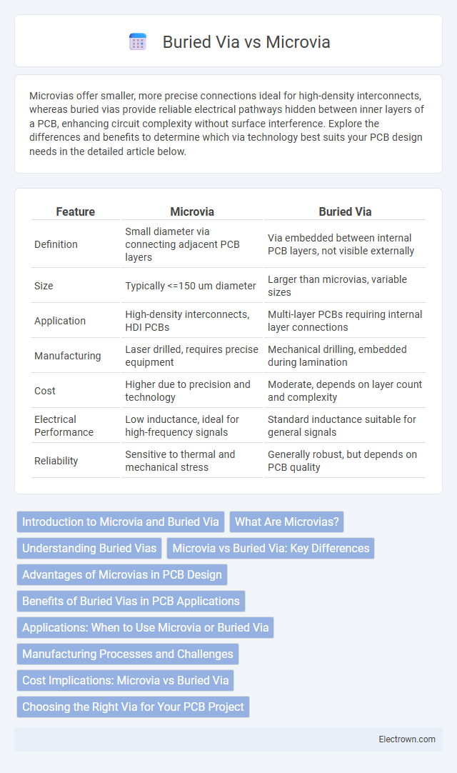
Table of Comparison
| Feature | Microvia | Buried Via |
|---|---|---|
| Definition | Small diameter via connecting adjacent PCB layers | Via embedded between internal PCB layers, not visible externally |
| Size | Typically <=150 um diameter | Larger than microvias, variable sizes |
| Application | High-density interconnects, HDI PCBs | Multi-layer PCBs requiring internal layer connections |
| Manufacturing | Laser drilled, requires precise equipment | Mechanical drilling, embedded during lamination |
| Cost | Higher due to precision and technology | Moderate, depends on layer count and complexity |
| Electrical Performance | Low inductance, ideal for high-frequency signals | Standard inductance suitable for general signals |
| Reliability | Sensitive to thermal and mechanical stress | Generally robust, but depends on PCB quality |
Introduction to Microvia and Buried Via
Microvias are small-diameter vias typically used in high-density interconnect (HDI) printed circuit boards (PCBs) to connect adjacent layers, allowing for greater circuit complexity and improved signal integrity. Buried vias, in contrast, are vias located entirely within the inner layers of a multilayer PCB and do not extend to the outer surfaces, providing enhanced layer-to-layer connectivity without occupying surface area. Both microvias and buried vias optimize PCB design by maximizing routing space and minimizing signal loss in advanced electronic applications.
What Are Microvias?
Microvias are tiny, laser-drilled holes in printed circuit boards (PCBs) that connect different layers, typically measuring less than 150 microns in diameter. Unlike buried vias, which are placed between inner layers and hidden from external layers, microvias offer higher density and improved electrical performance by enabling fine-pitch connections in high-speed and high-frequency PCB designs. Your choice of microvias enhances signal integrity and supports advanced miniaturization requirements in modern electronic devices.
Understanding Buried Vias
Buried vias are internal interconnections within a multilayer printed circuit board (PCB) that do not extend to the outer layers, enhancing signal integrity and saving surface space. Unlike microvias, which typically penetrate only one or two layers and are created using laser drilling, buried vias connect inner layers and are formed during the PCB lamination process. Their use is critical in high-density designs where maintaining compact layouts and minimizing electromagnetic interference are essential.
Microvia vs Buried Via: Key Differences
Microvias are small drilled holes that connect only adjacent layers in a multilayer PCB, typically less than 150 microns in diameter, while buried vias connect internal layers without extending to the surface, preserving surface area for component placement. Microvias enable higher density interconnections and are often used in HDI (High-Density Interconnect) boards, whereas buried vias support complex multilayer routing and reduce signal interference by isolating internal connections. The choice between microvia and buried via depends on design constraints like layer count, signal integrity, and manufacturing costs.
Advantages of Microvias in PCB Design
Microvias offer significant advantages in high-density PCB design, enabling finer circuit layouts with reduced signal path lengths that enhance electrical performance and reduce crosstalk. Their smaller size compared to buried vias allows for more efficient use of board space, supporting multi-layer stacking without compromising reliability. Microvias also improve thermal management by facilitating better heat dissipation in compact electronic devices.
Benefits of Buried Vias in PCB Applications
Buried vias enhance PCB design by enabling higher component density and improved signal integrity, as they connect internal layers without occupying surface space. Your circuits benefit from reduced electromagnetic interference and shorter signal paths, leading to faster data transmission and enhanced overall performance. This makes buried vias ideal for compact, high-frequency applications demanding reliability and efficient use of board real estate.
Applications: When to Use Microvia or Buried Via
Microvias are ideal for high-density interconnect (HDI) PCBs in smartphones and wearable devices, where space-saving and fine pitch are critical. Buried vias suit multilayer boards in complex electronics like automotive control units, providing interlayer connections without surface area consumption. You should choose microvias for compact, high-frequency circuits and buried vias for robust internal connectivity across multiple layers.
Manufacturing Processes and Challenges
Microvias are created using laser drilling or precision mechanical drilling followed by plating, allowing high-density interconnections in HDI PCBs with minimal space usage. Buried vias involve sequential lamination and drilling processes during multilayer PCB fabrication, presenting challenges such as accurate layer alignment and maintaining structural integrity between inner layers. Both require precise control of plating thickness and via aspect ratios to ensure electrical reliability and mechanical strength.
Cost Implications: Microvia vs Buried Via
Microvias generally incur higher costs due to advanced laser drilling technology and precise fabrication processes compared to buried vias, which are formed using traditional mechanical drilling methods. The smaller size and higher density capability of microvias contribute to increased manufacturing complexity and associated expenses, particularly in high-volume or multi-layer PCB production. Buried vias, while less expensive, limit routing flexibility and circuit density, potentially affecting overall design efficiency and long-term product cost-effectiveness.
Choosing the Right Via for Your PCB Project
Selecting the appropriate via type for your PCB project depends on factors such as board complexity, signal integrity, and manufacturing cost. Microvias offer high-density interconnections with minimal signal loss, ideal for HDI boards requiring finer pitch and layer-to-layer connections. Buried vias suit multi-layer PCBs by connecting internal layers without affecting surface routing, providing enhanced mechanical stability and reduced board size while typically lowering fabrication costs compared to microvias.
Microvia vs Buried Via Infographic