Open collector outputs use transistors that can only pull the line low, requiring an external pull-up resistor to achieve a high state, commonly found in TTL circuits. Open drain outputs function similarly but are associated with MOSFETs in CMOS technology, and understanding these differences can improve your circuit design; read on to explore their specific applications and benefits.
Table of Comparison
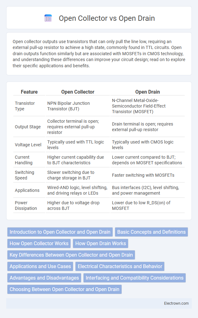
| Feature | Open Collector | Open Drain |
|---|---|---|
| Transistor Type | NPN Bipolar Junction Transistor (BJT) | N-Channel Metal-Oxide-Semiconductor Field-Effect Transistor (MOSFET) |
| Output Stage | Collector terminal is open; requires external pull-up resistor | Drain terminal is open; requires external pull-up resistor |
| Voltage Level | Typically used with TTL logic levels | Typically used with CMOS logic levels |
| Current Handling | Higher current capability due to BJT characteristics | Lower current compared to BJT; depends on MOSFET specifications |
| Switching Speed | Slower switching due to charge storage in BJT | Faster switching with MOSFETs |
| Applications | Wired-AND logic, level shifting, and driving relays or LEDs | Bus interfaces (I2C), level shifting, and power management |
| Power Dissipation | Higher due to voltage drop across BJT | Lower due to low R_DS(on) of MOSFET |
Introduction to Open Collector and Open Drain
Open collector and open drain are types of transistor output configurations commonly used for interfacing digital circuits. An open collector uses bipolar junction transistors (BJTs) to sink current but cannot source it, whereas an open drain employs MOSFET transistors with similar sinking properties. Your choice between open collector and open drain depends on the specific device technology and voltage level requirements in your circuit design.
Basic Concepts and Definitions
Open collector and open drain output configurations both refer to transistor-based interfaces used in digital circuits for wired-AND connections and level shifting. Open collector uses bipolar junction transistors (BJTs) with the collector terminal exposed for external connection, while open drain employs MOSFET transistors with the drain terminal accessible. These configurations require an external pull-up resistor to achieve a defined high logic level, allowing multiple devices to share a line without causing damage from conflicting outputs.
How Open Collector Works
Open collector works by using a transistor's collector terminal as an output that can either pull the line to ground or leave it floating, allowing external devices to control the voltage level with a pull-up resistor. This configuration enables multiple outputs to be wired together safely for wired-AND logic, which is crucial in bus systems and signal sharing applications. Your circuit benefits from open collector outputs because they provide flexible interfacing with different voltage levels and facilitate simple fault-tolerant communication.
How Open Drain Works
Open drain works by connecting the transistor's drain directly to the output pin, allowing it to either pull the line to ground (logic low) or leave it floating, relying on an external pull-up resistor to achieve logic high. This configuration enables multiple devices to share the same communication line without causing damage due to conflicting output states. Your circuit's design benefits from this by providing safe and efficient wired-AND logic for signals like I2C bus lines.
Key Differences Between Open Collector and Open Drain
Open collector and open drain configurations both refer to transistor output stages used in digital circuits, with open collector utilizing bipolar junction transistors (BJTs) and open drain employing metal-oxide-semiconductor field-effect transistors (MOSFETs). Key differences include voltage level compatibility, as open collector outputs are typically designed for TTL logic levels, while open drain outputs suit CMOS logic levels; pull-up resistor requirements also differ due to transistor characteristics. Open collector outputs can handle higher current loads but have slower switching speeds, whereas open drain outputs offer faster switching and lower power consumption, making them preferable in modern integrated circuits.
Applications and Use Cases
Open collector outputs are commonly employed in TTL logic circuits and transistor-transistor logic applications for wired-AND configurations and level shifting. Open drain outputs are predominantly used in I2C communication buses and other MOSFET-based systems, providing efficient voltage compatibility and multi-device bus connections. Both configurations excel in scenarios requiring flexible voltage interfacing and interrupt signaling in microcontroller applications.
Electrical Characteristics and Behavior
Open collector outputs use bipolar junction transistors and operate by sinking current to ground, allowing multiple outputs to be wired together for wired-AND logic. Open drain outputs employ MOSFET transistors and pull the line low when active, with a pull-up resistor determining the high state voltage level. Your choice between open collector and open drain depends on voltage levels, switching speed, and compatibility with the logic family used in your circuit.
Advantages and Disadvantages
Open collector outputs enable flexible interfacing with various voltage levels and allow multiple devices to connect via wired-AND logic, making them ideal for digital communication lines; however, they require external pull-up resistors, which can increase circuit complexity and power consumption. Open drain configurations function similarly but are commonly used with MOSFET transistors, offering low on-resistance and efficient switching, though they share the same limitation of needing pull-up resistors and can be slower due to the resistor-capacitor charging time. Both methods are advantageous for creating multiplexed or shared bus environments but may introduce slower signal rise times and increased pin count due to external components.
Interfacing and Compatibility Considerations
Open collector and open drain outputs both require external pull-up resistors for proper signal level interfacing, but open drain is commonly used with MOSFET transistors while open collector uses bipolar junction transistors, affecting their switching speed and voltage compatibility. Open collector outputs typically interface well with TTL logic levels, whereas open drain outputs are more compatible with modern CMOS technologies and I2C bus systems due to their ability to handle wider voltage ranges. Designers must consider these electrical characteristics and bus protocols to ensure reliable communication and avoid signal integrity issues in mixed-technology environments.
Choosing Between Open Collector and Open Drain
Choosing between open collector and open drain configurations depends on the type of transistor technology used: open collector circuits utilize bipolar junction transistors (BJTs), while open drain circuits use MOSFETs. You should consider voltage levels, switching speed, and power consumption requirements, as open drain typically offers faster switching and lower voltage drop due to MOSFET characteristics. Compatibility with the rest of your circuit, such as pull-up resistor values and logic levels, also influences the optimal choice for reliable communication and control.
Open collector vs open drain Infographic