Pull-up and pull-down networks are fundamental components in CMOS digital circuits, where the pull-up network typically consists of PMOS transistors that connect the output to the positive supply voltage, while the pull-down network uses NMOS transistors to connect the output to ground. Understanding how these complementary networks function and interact is crucial for optimizing your circuit design for speed, power, and reliability--explore the rest of the article to deepen your knowledge on this topic.
Table of Comparison
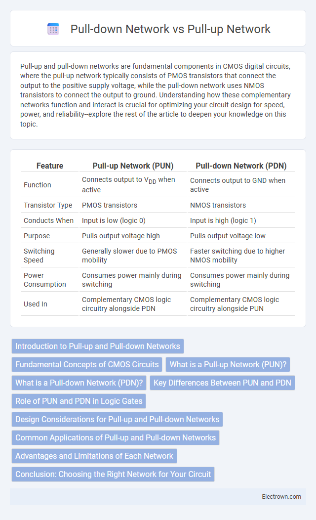
| Feature | Pull-up Network (PUN) | Pull-down Network (PDN) |
|---|---|---|
| Function | Connects output to VDD when active | Connects output to GND when active |
| Transistor Type | PMOS transistors | NMOS transistors |
| Conducts When | Input is low (logic 0) | Input is high (logic 1) |
| Purpose | Pulls output voltage high | Pulls output voltage low |
| Switching Speed | Generally slower due to PMOS mobility | Faster switching due to higher NMOS mobility |
| Power Consumption | Consumes power mainly during switching | Consumes power mainly during switching |
| Used In | Complementary CMOS logic circuitry alongside PDN | Complementary CMOS logic circuitry alongside PUN |
Introduction to Pull-up and Pull-down Networks
Pull-up and pull-down networks are fundamental components in CMOS logic design, responsible for driving the output voltage to the desired logic levels. Pull-up networks typically use PMOS transistors to connect the output to the power supply (VDD), ensuring a logic high level, while pull-down networks utilize NMOS transistors to connect the output to ground (GND), providing a logic low level. Understanding the complementary operation of these networks is crucial for optimizing circuit performance, power consumption, and reliability in digital integrated circuits.
Fundamental Concepts of CMOS Circuits
Pull-up and pull-down networks form the core of CMOS circuit operation, where the pull-up network typically uses p-type MOSFETs to connect the output to the positive voltage supply, ensuring a logic high level. The pull-down network, composed of n-type MOSFETs, connects the output to ground, producing a logic low level when activated. Your understanding of these complementary networks is crucial for designing energy-efficient, high-performance digital logic gates within CMOS technology.
What is a Pull-up Network (PUN)?
A Pull-up Network (PUN) is a type of transistor network used in CMOS logic circuits to connect the output node to the positive supply voltage (V_DD), ensuring the output voltage is pulled high when activated. It typically consists of PMOS transistors arranged to create a low-resistance path to V_DD when the input signals meet specific logic conditions. Understanding the structure and function of your PUN is crucial for designing efficient digital circuits, as it directly influences output drive capability and power consumption.
What is a Pull-down Network (PDN)?
A Pull-down Network (PDN) is a critical component in CMOS logic circuits designed to connect the output node to ground when activated, enabling a logic '0' output. Comprised primarily of NMOS transistors arranged in series or parallel, the PDN ensures efficient discharge of the output node, providing fast and reliable switching performance. The PDN's complementary function to the Pull-up Network (PUN) optimizes power consumption and noise margins in digital circuit design.
Key Differences Between PUN and PDN
Pull-up networks (PUN) use PMOS transistors to connect the output to the positive voltage supply, enabling a strong logic high output, while pull-down networks (PDN) use NMOS transistors to connect the output to ground, ensuring a strong logic low output. PUN typically consumes less static power during logic high due to the high resistance of PMOS transistors when off, whereas PDN efficiently pulls the output to ground during logic low with higher electron mobility in NMOS devices. The complementary design of PUN and PDN in CMOS circuits balances speed, power, and noise margins, crucial for optimized digital logic gate performance.
Role of PUN and PDN in Logic Gates
The Pull-up Network (PUN) and Pull-down Network (PDN) form the fundamental components of CMOS logic gates, where the PUN typically consists of PMOS transistors that connect the output to the power supply during logic high states. The PDN includes NMOS transistors that connect the output to ground during logic low states, ensuring complementary switching and low power consumption. Together, PUN and PDN enable fast switching, noise immunity, and reduce static power dissipation by ensuring that only one network conducts at a time during logic transitions.
Design Considerations for Pull-up and Pull-down Networks
Design considerations for pull-up and pull-down networks revolve around balancing switching speed, power consumption, and noise margins in CMOS circuits. Pull-up networks typically use PMOS transistors optimized for slower but low-leakage current, while pull-down networks use NMOS transistors favored for faster switching and stronger drive capability. Your circuit's performance and power efficiency depend on careful transistor sizing and threshold voltage selection to ensure reliable logic level transitions without excessive power dissipation.
Common Applications of Pull-up and Pull-down Networks
Pull-up and pull-down networks are essential in CMOS logic circuits, where pull-up networks connect outputs to the positive supply voltage, typically using PMOS transistors, and pull-down networks connect outputs to ground, usually with NMOS transistors. Common applications include digital logic gates, such as inverters, NAND, and NOR gates, where pull-up networks ensure high output levels and pull-down networks drive outputs low based on input signals. Understanding these networks helps you design efficient switching circuits with low power consumption and high noise margins.
Advantages and Limitations of Each Network
Pull-up networks, typically composed of PMOS transistors, offer low static power consumption and robust output drive capabilities, making them ideal for sourcing current to the output. Their limitations include slower switching speeds due to the lower mobility of holes in PMOS devices and increased area consumption on silicon. In contrast, pull-down networks, formed with NMOS transistors, provide faster switching speeds and smaller device size because of the higher electron mobility in NMOS but suffer from higher static power dissipation and weaker ability to pull the output high.
Conclusion: Choosing the Right Network for Your Circuit
Selecting the appropriate network between pull-up and pull-down depends on circuit requirements such as voltage levels, noise immunity, and power consumption. Pull-up networks are ideal for ensuring a default high state and are commonly used in open-drain or open-collector configurations. Pull-down networks effectively maintain a default low state, preventing floating inputs and enhancing signal stability in digital logic circuits.
Pull-up Network vs Pull-down Network Infographic