Solder bumps and Ball Grid Arrays (BGAs) are crucial components in semiconductor packaging, where solder bumps serve as tiny soldered connections between ICs and substrates, while BGAs refer to the overall package incorporating an array of these solder balls for enhanced electrical performance and thermal management. Understanding the differences can improve Your choice of packaging technology for reliability and assembly efficiency; explore further to learn the key advantages and applications of each.
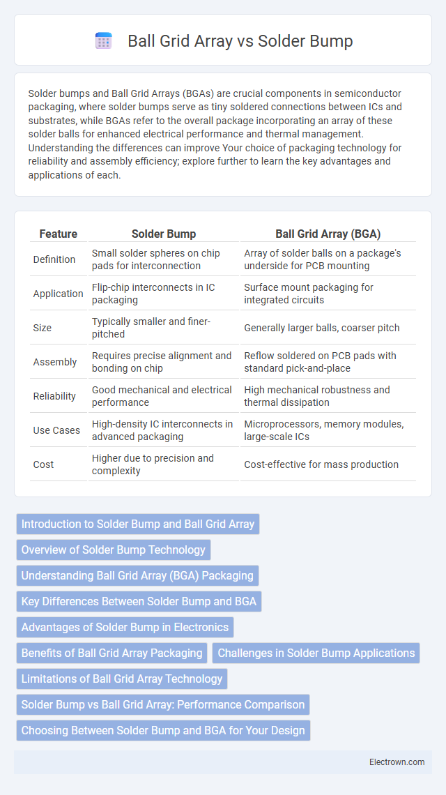
Table of Comparison
| Feature | Solder Bump | Ball Grid Array (BGA) |
|---|---|---|
| Definition | Small solder spheres on chip pads for interconnection | Array of solder balls on a package's underside for PCB mounting |
| Application | Flip-chip interconnects in IC packaging | Surface mount packaging for integrated circuits |
| Size | Typically smaller and finer-pitched | Generally larger balls, coarser pitch |
| Assembly | Requires precise alignment and bonding on chip | Reflow soldered on PCB pads with standard pick-and-place |
| Reliability | Good mechanical and electrical performance | High mechanical robustness and thermal dissipation |
| Use Cases | High-density IC interconnects in advanced packaging | Microprocessors, memory modules, large-scale ICs |
| Cost | Higher due to precision and complexity | Cost-effective for mass production |
Introduction to Solder Bump and Ball Grid Array
Solder bumps are tiny metallic spheres used to create electrical connections between semiconductor devices and substrates in advanced packaging technologies. Ball Grid Array (BGA) is a packaging type that arranges solder bumps in a grid pattern on the underside of integrated circuits, offering enhanced thermal and electrical performance. Your choice between solder bump types and BGA configurations depends on factors like device complexity, heat dissipation needs, and manufacturing capabilities.
Overview of Solder Bump Technology
Solder bump technology involves tiny, precisely deposited solder spheres used to create electrical connections between semiconductor devices and substrates, enabling reliable microelectronic packaging. This technique underpins Ball Grid Array (BGA) assemblies, where solder bumps form the electrical interface arranged in a matrix pattern on the chip's surface. The precise control over solder bump size, composition, and placement is critical for ensuring signal integrity, mechanical strength, and thermal performance in high-density integrated circuits.
Understanding Ball Grid Array (BGA) Packaging
Ball Grid Array (BGA) packaging features solder bumps arranged in a grid pattern on the underside of an integrated circuit, providing enhanced electrical performance and efficient heat dissipation compared to traditional leads. These solder bumps are significantly smaller and more densely packed than standard solder bumps, allowing for higher pin counts and improved signal integrity in compact applications. The BGA design enables robust mechanical connections and reduces inductance, making it ideal for advanced microprocessor and memory devices requiring reliable surface-mount solder joints.
Key Differences Between Solder Bump and BGA
Solder bump technology involves tiny solder spheres used primarily for direct chip-to-substrate connections, whereas Ball Grid Array (BGA) incorporates these solder bumps arranged in a grid pattern on the package underside for high-density interconnections. Key differences include the scale and application; solder bumps are essential components of BGA and Chip Scale Packages (CSP), while BGAs refer to the complete packaging format that utilizes an array of solder bumps for improved electrical performance and thermal dissipation. BGAs support higher pin counts and more robust mechanical integrity compared to discrete solder bumps, which serve as fundamental solder joints in various microelectronics assembly processes.
Advantages of Solder Bump in Electronics
Solder bumps provide precise and reliable electrical connections in advanced semiconductor packaging, enabling higher input/output (I/O) density compared to traditional wire bonding methods. Their small size and excellent thermal conductivity improve heat dissipation and signal integrity, essential for high-frequency electronic devices. Solder bump technology enhances mechanical strength and reduces package size, facilitating miniaturization in mobile and wearable electronics.
Benefits of Ball Grid Array Packaging
Ball Grid Array (BGA) packaging offers superior electrical performance and thermal efficiency compared to traditional solder bump techniques, enabling higher density interconnections and enhanced signal integrity. The distributed array of solder balls allows for improved heat dissipation, reducing the risk of thermal damage and increasing the reliability of high-performance electronic devices. BGA packaging also facilitates easier automated assembly and testing, leading to enhanced manufacturing yield and cost-effectiveness in complex semiconductor applications.
Challenges in Solder Bump Applications
Solder bump applications face significant challenges including precise alignment and controlling solder volume to prevent bridging or open circuits in Ball Grid Array (BGA) assemblies. Thermal stress during reflow soldering can cause mechanical failures and reliability issues due to differing material expansion rates. Your ability to manage these factors is critical to ensuring consistent electrical performance and long-term durability in advanced electronic packaging.
Limitations of Ball Grid Array Technology
Ball Grid Array (BGA) technology faces limitations such as difficulties in rework and inspection due to its hidden solder joints underneath the package, which complicates visual inspection and repair processes. Thermal expansion mismatches between the BGA substrate and PCB can cause solder joint fatigue, leading to reliability issues in high-stress environments. Additionally, BGA packages require precise alignment during assembly, increasing manufacturing complexity and cost compared to simpler solder bump techniques.
Solder Bump vs Ball Grid Array: Performance Comparison
Solder bumps provide precise, low-resistance connections essential for high-frequency signal transmission, while Ball Grid Arrays (BGAs) offer enhanced mechanical stability and superior heat dissipation due to their distinct ball-shaped interconnects. Performance-wise, solder bumps excel in fine-pitch applications requiring minimal parasitic inductance, whereas BGAs support higher pin counts and improved reliability under thermal cycling. Your choice between solder bump and BGA technologies should weigh these factors against the specific electrical and thermal demands of your device.
Choosing Between Solder Bump and BGA for Your Design
Selecting between solder bump and ball grid array (BGA) technologies depends on the design's size, performance, and reliability requirements. Solder bumps offer fine pitch connections ideal for high-density, compact semiconductor packaging, improving electrical performance and thermal dissipation. BGAs provide robust mechanical stability and ease of assembly for larger, more complex integrated circuits, balancing cost and manufacturability in advanced electronic applications.
Solder Bump vs Ball Grid Array Infographic