QFN (Quad Flat No-Lead) packages offer excellent thermal performance and robust mechanical stability, making them ideal for applications requiring efficient heat dissipation and reliable soldering. Explore the rest of the article to understand how WLCSP (Wafer-Level Chip Scale Package) compares in terms of size, cost, and electrical performance for your next project.
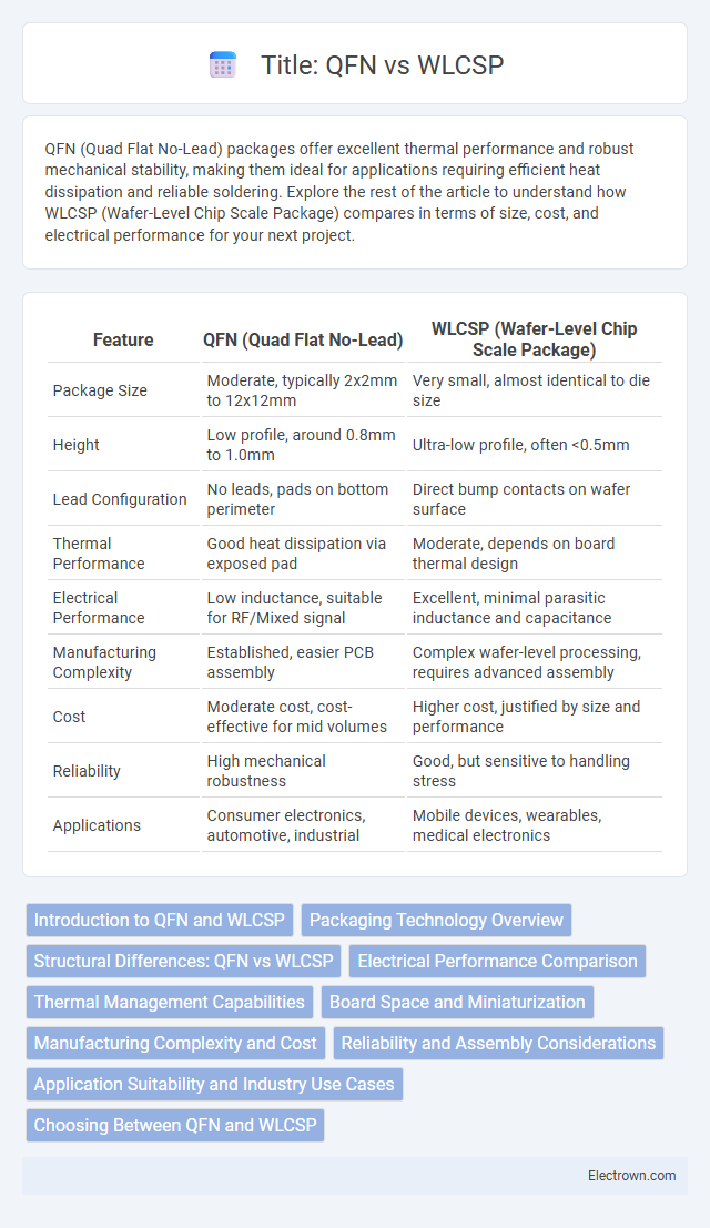
Table of Comparison
| Feature | QFN (Quad Flat No-Lead) | WLCSP (Wafer-Level Chip Scale Package) |
|---|---|---|
| Package Size | Moderate, typically 2x2mm to 12x12mm | Very small, almost identical to die size |
| Height | Low profile, around 0.8mm to 1.0mm | Ultra-low profile, often <0.5mm |
| Lead Configuration | No leads, pads on bottom perimeter | Direct bump contacts on wafer surface |
| Thermal Performance | Good heat dissipation via exposed pad | Moderate, depends on board thermal design |
| Electrical Performance | Low inductance, suitable for RF/Mixed signal | Excellent, minimal parasitic inductance and capacitance |
| Manufacturing Complexity | Established, easier PCB assembly | Complex wafer-level processing, requires advanced assembly |
| Cost | Moderate cost, cost-effective for mid volumes | Higher cost, justified by size and performance |
| Reliability | High mechanical robustness | Good, but sensitive to handling stress |
| Applications | Consumer electronics, automotive, industrial | Mobile devices, wearables, medical electronics |
Introduction to QFN and WLCSP
QFN (Quad Flat No-Lead) and WLCSP (Wafer-Level Chip-Scale Package) are advanced semiconductor packaging technologies designed for high-performance electronic devices. QFN offers a compact, leadless surface-mount package with excellent thermal and electrical performance, while WLCSP integrates the chip directly onto the package, minimizing size and improving signal integrity. Understanding the strengths of QFN and WLCSP can help optimize your device's reliability and functionality in space-constrained applications.
Packaging Technology Overview
QFN (Quad Flat No-Lead) and WLCSP (Wafer-Level Chip-Scale Package) are advanced semiconductor packaging technologies designed to optimize device performance and form factor. QFN provides a low-profile, thermally efficient package with external contacts along the edges, offering robust mechanical stability and superior heat dissipation for mid- to high-performance applications. WLCSP enables direct chip-level packaging with minimal footprint and parasitic inductance, ideal for ultra-compact devices requiring high electrical performance and cost-effective mass production.
Structural Differences: QFN vs WLCSP
QFN (Quad Flat No-Lead) packages feature a rectangular or square plastic body with metal pads exposed on the bottom edges for soldering, providing excellent thermal performance and mechanical strength. WLCSP (Wafer-Level Chip Scale Package) is a chip-scale package where the die is directly covered by redistribution layers (RDL) and solder bumps, resulting in a much smaller footprint with superior electrical performance. The primary structural difference lies in QFN's molded encapsulation with lead frames versus WLCSP's wafer-level fabrication with no encapsulating body, influencing their applications in high-density, space-constrained electronics.
Electrical Performance Comparison
QFN (Quad Flat No-Lead) packages offer superior thermal dissipation and lower inductance due to their exposed pad design, enhancing high-frequency electrical performance. WLCSP (Wafer-Level Chip Scale Package) provides minimal parasitic resistance and capacitance by eliminating wire bonds, resulting in excellent signal integrity at very high frequencies. Your choice depends on the specific requirements for signal speed, thermal management, and board space in your electronic design.
Thermal Management Capabilities
QFN packages offer superior thermal management capabilities due to their exposed die paddle, which efficiently dissipates heat through the PCB, making them ideal for high-power applications. In contrast, WLCSP relies on the silicon wafer itself for heat dissipation, resulting in less effective thermal conductivity and potential hotspots under heavy load. Optimal thermal performance in QFN supports higher current densities and longer device reliability compared to the more compact but thermally constrained WLCSP.
Board Space and Miniaturization
QFN (Quad Flat No-lead) packages offer a compact footprint but generally occupy more board space compared to WLCSP (Wafer-Level Chip Scale Package), which is designed for extreme miniaturization with the smallest possible form factor. WLCSP enables direct die attachment on the PCB, eliminating the need for traditional packaging and significantly reducing the overall device size. This makes WLCSP ideal for applications demanding ultra-compact designs and high-density board layouts.
Manufacturing Complexity and Cost
QFN (Quad Flat No-lead) packaging typically involves moderate manufacturing complexity due to its exposed paddle design that requires precise soldering and inspection processes. WLCSP (Wafer Level Chip Scale Package) offers reduced footprint and higher integration but demands advanced wafer thinning, dicing, and underfill techniques, increasing production complexity and cost significantly. Your choice between QFN and WLCSP will impact assembly line requirements and overall budget, with WLCSP generally incurring higher expenses due to its intricate wafer-level processing.
Reliability and Assembly Considerations
QFN (Quad Flat No-lead) packages offer robust mechanical reliability due to their exposed paddle that enhances thermal dissipation and solder joint strength, making them suitable for high-stress applications. WLCSP (Wafer-Level Chip Scale Package) provides superior electrical performance and miniaturization but requires precise assembly processes to mitigate risks related to die warpage and sensitive solder bump integrity. Careful consideration of reflow profiles and board surface finishes is critical to optimize solder joint reliability for both QFN and WLCSP packaging technologies.
Application Suitability and Industry Use Cases
QFN (Quad Flat No-Lead) packages excel in high-performance applications requiring robust thermal management and mechanical stability, making them ideal for automotive, telecommunications, and industrial electronics. WLCSP (Wafer-Level Chip Scale Package) suits compact consumer electronics like smartphones and wearables due to its minimal footprint and improved electrical performance. Your choice depends on application demands for durability and size, aligning QFN with rugged environments and WLCSP with space-constrained designs.
Choosing Between QFN and WLCSP
Choosing between QFN (Quad Flat No-lead) and WLCSP (Wafer-Level Chip Scale Package) depends on your design priorities such as size, thermal performance, and cost. QFN offers excellent thermal and electrical performance with good mechanical robustness, making it suitable for power-sensitive applications. WLCSP provides a smaller footprint and lower inductance, ideal for ultra-compact devices where board space is critical.
QFN vs WLCSP Infographic