NMOS passgates allow signals to pass when the gate voltage is high but suffer from a threshold voltage drop, leading to degraded signal levels in certain conditions. Understanding the differences between NMOS passgates and transmission gates can help you choose the right component for your circuit design; read on to explore their advantages and applications.
Table of Comparison
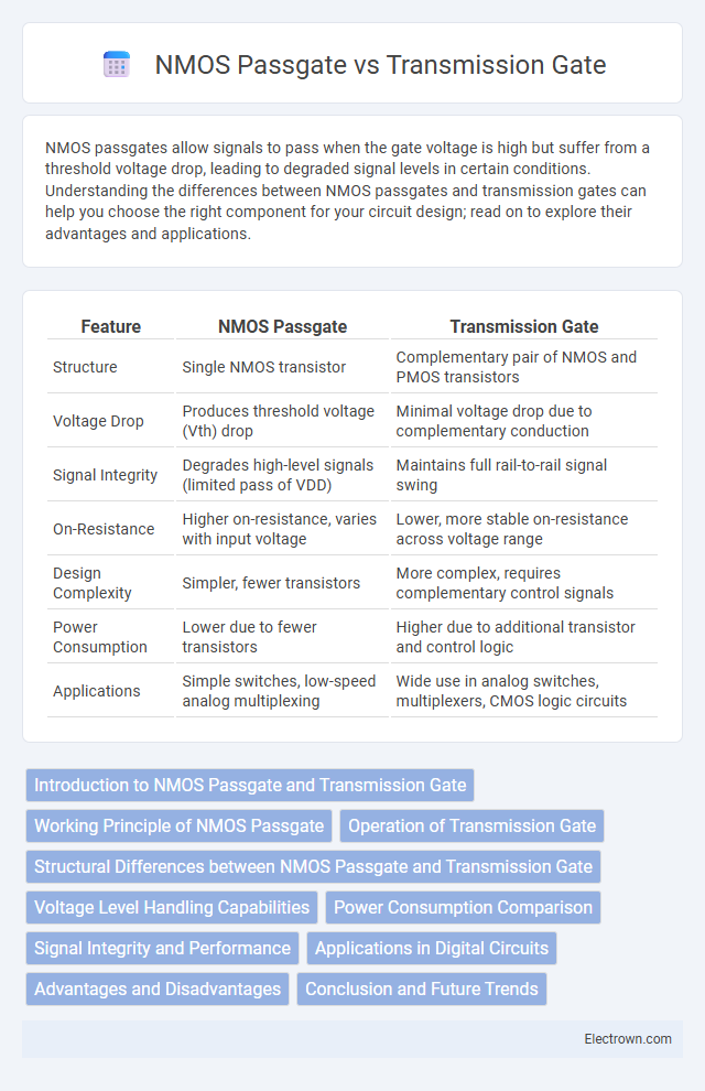
| Feature | NMOS Passgate | Transmission Gate |
|---|---|---|
| Structure | Single NMOS transistor | Complementary pair of NMOS and PMOS transistors |
| Voltage Drop | Produces threshold voltage (Vth) drop | Minimal voltage drop due to complementary conduction |
| Signal Integrity | Degrades high-level signals (limited pass of VDD) | Maintains full rail-to-rail signal swing |
| On-Resistance | Higher on-resistance, varies with input voltage | Lower, more stable on-resistance across voltage range |
| Design Complexity | Simpler, fewer transistors | More complex, requires complementary control signals |
| Power Consumption | Lower due to fewer transistors | Higher due to additional transistor and control logic |
| Applications | Simple switches, low-speed analog multiplexing | Wide use in analog switches, multiplexers, CMOS logic circuits |
Introduction to NMOS Passgate and Transmission Gate
NMOS Passgate is a single n-channel MOSFET used as a switch to pass signals, but it suffers from threshold voltage drop, limiting its effectiveness in passing high-level signals. Transmission Gate combines both NMOS and PMOS transistors in parallel, allowing it to pass both high and low voltage levels more efficiently by overcoming the threshold voltage issue. This complementary structure of the Transmission Gate results in lower resistance and better signal integrity compared to a standalone NMOS Passgate.
Working Principle of NMOS Passgate
The NMOS passgate functions by allowing electrons to flow from the source to the drain when the gate voltage is sufficiently high, effectively acting as a switch controlled by the gate terminal. It passes a strong logic '0' but experiences threshold voltage drop when passing a logic '1,' which limits its output level and causes signal degradation. This voltage drop is due to the inherent threshold voltage (Vth) of the NMOS transistor, making it less efficient for passing a high-level signal compared to transmission gates.
Operation of Transmission Gate
A transmission gate operates by using both NMOS and PMOS transistors connected in parallel to pass digital signals with minimal voltage degradation, enabling full rail-to-rail voltage swing. Unlike a single NMOS passgate that suffers from a threshold voltage drop when conveying high logic levels, the complementary arrangement in a transmission gate ensures low on-resistance and symmetric conduction for both high and low input signals. This bidirectional switching capability and reduced signal distortion make transmission gates essential in analog multiplexers, data selectors, and bus switches.
Structural Differences between NMOS Passgate and Transmission Gate
NMOS passgates consist of a single NMOS transistor that conducts well when passing a low voltage but suffers from reduced signal levels when transmitting a high voltage due to threshold voltage drop. Transmission gates combine both NMOS and PMOS transistors in parallel, allowing efficient conduction of both high and low signals without significant voltage loss. Your circuit performance improves with transmission gates by leveraging this complementary transistor structure for more reliable signal transmission.
Voltage Level Handling Capabilities
NMOS pass gates suffer from threshold voltage drop, limiting their voltage level handling capabilities by reducing the output voltage close to VDD - Vth. Transmission gates, combining NMOS and PMOS transistors, effectively eliminate this threshold drop, enabling full rail-to-rail voltage transmission without degradation. This characteristic makes transmission gates superior for applications requiring precise voltage level handling in analog and digital circuits.
Power Consumption Comparison
NMOS passgates typically consume less static power due to their simpler structure but suffer from threshold voltage drops causing signal degradation and potential leakage currents. Transmission gates, combining NMOS and PMOS transistors, offer lower on-resistance and reduced signal loss, optimizing dynamic power consumption during switching. Your choice between the two should balance power efficiency and signal integrity, with transmission gates generally providing better overall power performance in CMOS circuits.
Signal Integrity and Performance
NMOS passgates suffer from threshold voltage drops that degrade signal integrity, especially in low-voltage applications, causing a reduced high-level output voltage. Transmission gates, composed of parallel NMOS and PMOS transistors, provide full rail-to-rail swing, preserving signal integrity and minimizing voltage degradation. Your circuits benefit from improved performance and reliability when using transmission gates due to their superior switching characteristics and reduced resistance.
Applications in Digital Circuits
NMOS passgates are commonly used for simple switching applications where reduced area and lower complexity are critical, typically found in signal gating and level shifting circuits. Transmission gates, which combine NMOS and PMOS transistors, offer better voltage swing and reduced on-resistance, making them ideal for multiplexers, flip-flops, and analog switches in digital circuits. Your design choice depends on the trade-off between performance and power consumption requirements.
Advantages and Disadvantages
NMOS passgates offer simpler design and faster switching speeds but suffer from threshold voltage drop, causing signal degradation in low-voltage applications. Transmission gates, combining NMOS and PMOS transistors, provide full voltage swing and improved signal integrity but require more area and higher complexity. While NMOS passgates excel in speed and area efficiency, transmission gates ensure better performance with minimal voltage loss, making them ideal for precise analog and digital switching.
Conclusion and Future Trends
NMOS passgates exhibit simpler design and lower transistor count but suffer from threshold voltage drop and limited signal swing, impacting overall performance in analog and digital circuits. Transmission gates leverage complementary NMOS and PMOS transistors to provide near rail-to-rail pass characteristics, enabling superior signal integrity and reduced distortion, making them the standard in high-performance switching applications. Future trends emphasize scaling challenges at nanometer technologies, promoting the integration of advanced materials and adaptive control schemes to optimize transmission gate efficiency and reliability in emerging low-power and high-frequency systems.
NMOS Passgate vs Transmission Gate Infographic