SOI technology offers reduced parasitic capacitance and improved performance compared to Bulk CMOS, leading to lower power consumption and better speed for your semiconductor devices. Explore the rest of the article to understand the detailed advantages and applications of SOI versus Bulk CMOS.
Table of Comparison
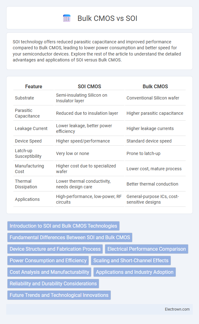
| Feature | SOI CMOS | Bulk CMOS |
|---|---|---|
| Substrate | Semi-insulating Silicon on Insulator layer | Conventional Silicon wafer |
| Parasitic Capacitance | Reduced due to insulation layer | Higher parasitic capacitance |
| Leakage Current | Lower leakage, better power efficiency | Higher leakage currents |
| Device Speed | Higher speed/performance | Standard device speed |
| Latch-up Susceptibility | Very low or none | Prone to latch-up |
| Manufacturing Cost | Higher cost due to specialized wafer | Lower cost, mature process |
| Thermal Dissipation | Lower thermal conductivity, needs design care | Better thermal conduction |
| Applications | High-performance, low-power, RF circuits | General-purpose ICs, cost-sensitive designs |
Introduction to SOI and Bulk CMOS Technologies
SOI (Silicon-On-Insulator) technology integrates a thin layer of silicon atop an insulating substrate, reducing parasitic capacitance and enhancing device speed and power efficiency. Bulk CMOS, built directly on a silicon wafer, remains widely used due to lower fabrication costs and mature process technology. SOI offers significant advantages in leakage current reduction and radiation hardness, making it ideal for high-performance and low-power applications compared to conventional Bulk CMOS devices.
Fundamental Differences Between SOI and Bulk CMOS
SOI (Silicon-On-Insulator) technology features a thin silicon layer separated from the substrate by an insulating oxide layer, significantly reducing parasitic capacitance and improving performance. Bulk CMOS is fabricated on a single crystalline silicon substrate, where devices share the same silicon bulk, leading to higher substrate coupling and leakage currents. The fundamental distinction lies in SOI's insulated silicon layer offering enhanced isolation and reduced short-channel effects compared to the continuous silicon in bulk CMOS.
Device Structure and Fabrication Process
SOI (Silicon-on-Insulator) technology features a layered device structure with a thin silicon layer atop an insulating oxide layer, reducing parasitic capacitance and improving performance compared to traditional bulk CMOS, which uses a silicon substrate without an insulating layer. SOI fabrication involves bonding a thin silicon film to an insulator followed by precise thinning and doping processes, while bulk CMOS fabrication relies on doping directly into the silicon substrate and forming junctions without an oxide insulating layer beneath the active devices. The SOI structure minimizes leakage currents and short-channel effects, making it advantageous for high-speed and low-power applications compared to bulk CMOS.
Electrical Performance Comparison
SOI (Silicon-On-Insulator) technology offers superior electrical performance compared to bulk CMOS due to reduced parasitic capacitance and leakage currents, resulting in faster switching speeds and lower power consumption. The buried oxide layer in SOI devices significantly improves short-channel control and reduces latch-up susceptibility, enhancing device reliability and scalability in advanced nodes. Bulk CMOS, while more cost-effective, typically exhibits higher junction capacitance and substrate coupling, which can degrade signal integrity and limit performance in high-frequency applications.
Power Consumption and Efficiency
SOI CMOS technology significantly reduces power consumption by minimizing parasitic capacitance and leakage currents compared to Bulk CMOS, leading to enhanced energy efficiency in high-performance and low-power applications. The buried oxide layer in SOI acts as an insulator, which improves switching speed and reduces dynamic power dissipation, making it suitable for mobile and battery-operated devices. In contrast, Bulk CMOS devices typically exhibit higher stand-by power and slower switching speeds due to substrate losses and greater junction capacitances.
Scaling and Short-Channel Effects
SOI technology offers superior scaling advantages over Bulk CMOS by reducing parasitic capacitance and leakage currents, which enhances transistor performance at smaller nodes. The buried oxide layer in SOI effectively suppresses short-channel effects (SCE) such as drain-induced barrier lowering (DIBL) and threshold voltage roll-off, enabling more aggressive device miniaturization. Bulk CMOS faces increased SCE challenges due to body doping variations and junction leakage, limiting its scaling potential compared to SOI-based transistors.
Cost Analysis and Manufacturability
SOI (Silicon-On-Insulator) technology generally incurs higher fabrication costs compared to Bulk CMOS due to complex wafer processing and specialized substrate requirements. However, SOI offers improved device performance and power efficiency, potentially reducing overall system costs in high-performance applications. Bulk CMOS remains more cost-effective and widely manufacturable for large-scale production due to mature fabrication infrastructure and lower material expenses.
Applications and Industry Adoption
SOI technology is widely favored in RF applications, high-performance computing, and low-power devices due to its superior speed, reduced parasitic capacitance, and better thermal management. Bulk CMOS remains dominant in cost-sensitive mass-market applications such as microcontrollers, sensors, and general-purpose logic due to its lower manufacturing expenses and established supply chains. Your choice between SOI and Bulk CMOS will depend on balancing performance requirements against cost constraints and the specific demands of the target industry.
Reliability and Durability Considerations
SOI (Silicon-On-Insulator) technology offers superior reliability and durability compared to Bulk CMOS due to its inherent isolation from substrate noise and reduced parasitic capacitance, which minimize latch-up and leakage currents. The buried oxide layer in SOI devices enhances tolerance to radiation and thermal stress, extending device lifespan in harsh environments. Choosing SOI for your applications can significantly improve performance stability and longevity under demanding operating conditions.
Future Trends and Technological Innovations
SOI (Silicon on Insulator) technology is advancing with innovations in ultra-thin BOX (Buried Oxide) layers and fully depleted SOI architectures, enhancing power efficiency and reducing parasitic capacitance for future low-power applications. Bulk CMOS is evolving through FD-SOI (Fully Depleted SOI)-like techniques and advanced strain engineering to improve transistor performance and scaling, supporting high-volume, cost-effective manufacturing. Your choice between SOI and Bulk CMOS will depend on the need for cutting-edge power management versus mature, scalable solutions in emerging semiconductor technologies.
SOI vs Bulk CMOS Infographic