Pad Limited design focuses on restricting electrical loading and routing paths to improve signal integrity in printed circuit boards, while Core Limited design prioritizes controlling the substrate's dielectric properties to enhance overall PCB performance. Explore the rest of the article to understand how these design approaches can impact Your electronic device's reliability and efficiency.
Table of Comparison
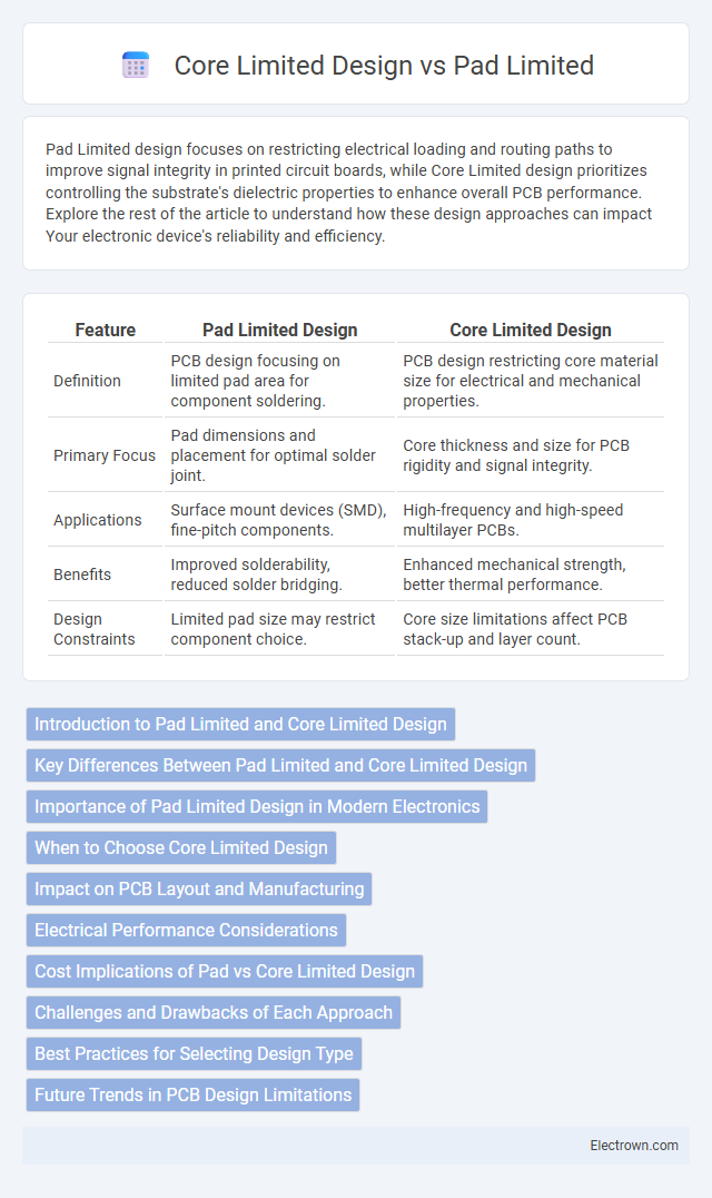
| Feature | Pad Limited Design | Core Limited Design |
|---|---|---|
| Definition | PCB design focusing on limited pad area for component soldering. | PCB design restricting core material size for electrical and mechanical properties. |
| Primary Focus | Pad dimensions and placement for optimal solder joint. | Core thickness and size for PCB rigidity and signal integrity. |
| Applications | Surface mount devices (SMD), fine-pitch components. | High-frequency and high-speed multilayer PCBs. |
| Benefits | Improved solderability, reduced solder bridging. | Enhanced mechanical strength, better thermal performance. |
| Design Constraints | Limited pad size may restrict component choice. | Core size limitations affect PCB stack-up and layer count. |
Introduction to Pad Limited and Core Limited Design
Pad Limited Design minimizes the placement of conductive pads directly on the PCB surface to reduce parasitic capacitance and noise interference, enhancing signal integrity in high-frequency circuits. Core Limited Design restricts the use of core materials only to essential regions within multilayer PCBs, optimizing mechanical stability while controlling costs and weight. Understanding these approaches helps you select the best PCB design strategy for balancing electrical performance and manufacturing constraints.
Key Differences Between Pad Limited and Core Limited Design
Pad limited design focuses on maximizing the use of available pad area for circuit layout, often prioritizing component placement over routing flexibility. Core limited design prioritizes efficient routing within the core layers of the PCB, enabling higher signal density and improved electrical performance. Understanding these distinctions helps you choose the optimal design strategy based on whether pad space or core routing complexity is the critical constraint in your project.
Importance of Pad Limited Design in Modern Electronics
Pad Limited Design is crucial in modern electronics because it ensures precise placement and efficient use of limited solder pad space, optimizing component density on printed circuit boards (PCBs). This design approach enhances signal integrity and thermal management by minimizing pad size and reducing parasitic effects common in high-frequency circuits. Efficient Pad Limited Design drives advancements in miniaturization and reliability for compact, high-performance electronic devices.
When to Choose Core Limited Design
Core Limited Design is ideal when minimizing die size and reducing manufacturing costs are primary goals, especially in high-volume semiconductor production. This approach limits the number of I/O pads to critical signals, optimizing chip real estate for complex core functionality without the overhead of extensive external connections. Selecting Core Limited Design is preferable in applications where packaging constraints and power efficiency outweigh the need for extensive I/O interfacing.
Impact on PCB Layout and Manufacturing
Pad Limited design restricts copper areas precisely to the size of the pad, minimizing solder mask exposure and reducing solder bridging risks, which enhances manufacturing yield and reliability. Core Limited design allows larger copper areas than the pad size on the core layer, improving thermal dissipation but increasing the complexity of PCB etching and potential for solder shorts. Choosing between Pad Limited and Core Limited significantly affects PCB layout precision, solder mask application, and overall manufacturing cost efficiency.
Electrical Performance Considerations
Pad Limited Design enhances electrical performance by minimizing parasitic capacitance through reduced pad size, leading to improved signal integrity and faster switching speeds. Core Limited Design, by maintaining a larger core area, may introduce increased resistance and capacitance, potentially causing signal delay and power loss. Your choice depends on balancing these factors to optimize overall circuit efficiency and reliability.
Cost Implications of Pad vs Core Limited Design
Pad Limited Design typically incurs lower manufacturing costs due to simpler wafer fabrication processes and reduced material usage. Core Limited Design often leads to higher initial expenses because of complex integration and greater demand for high-precision lithography, but it can optimize performance for specific applications. Cost implications must balance immediate expenditure with long-term efficiency gains inherent to each design approach.
Challenges and Drawbacks of Each Approach
Pad Limited Design faces challenges such as increased PCB area and routing complexity, leading to higher manufacturing costs and potential signal integrity issues. Core Limited Design suffers from thermal management difficulties and limited layer scalability, which can restrict the performance and reliability of high-density electronic devices. Both approaches require trade-offs between manufacturing feasibility, electrical performance, and cost efficiency in PCB production.
Best Practices for Selecting Design Type
Selecting between pad limited and core limited design hinges on optimizing memory usage and power efficiency in integrated circuits. Best practices emphasize evaluating the critical path and timing constraints to determine if pads, which handle input/output functions, or cores, which manage internal logic, dominate performance bottlenecks. Prioritizing core limited design suits applications demanding high internal processing speed, whereas pad limited design benefits scenarios requiring robust input/output handling and signal integrity.
Future Trends in PCB Design Limitations
Future trends in PCB design highlight the shift from traditional Pad Limited layouts, where component pads dominate the routing space, toward Core Limited designs emphasizing controlled impedance and signal integrity within the PCB core layers. Advances in high-speed digital applications and miniaturization demand PCB architectures that minimize crosstalk and electromagnetic interference, favoring Core Limited designs that optimize internal layer configurations. Your next PCB project should consider these evolving constraints to ensure performance scalability and adherence to tighter manufacturing tolerances.
Pad Limited vs Core Limited Design Infographic