Electrostatic Discharge (ESD) causes sudden, high-voltage spikes that can damage sensitive electronic components, whereas latchup is a condition where a parasitic structure within a semiconductor device creates a low-resistance path, leading to device failure or burnout. Understanding the differences between ESD and latchup is crucial for protecting your circuits effectively--read on to explore the detailed distinctions and prevention methods.
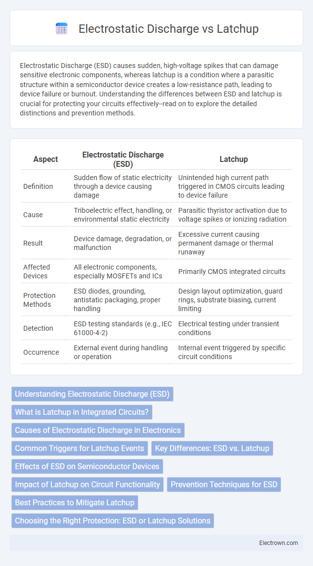
Table of Comparison
| Aspect | Electrostatic Discharge (ESD) | Latchup |
|---|---|---|
| Definition | Sudden flow of static electricity through a device causing damage | Unintended high current path triggered in CMOS circuits leading to device failure |
| Cause | Triboelectric effect, handling, or environmental static electricity | Parasitic thyristor activation due to voltage spikes or ionizing radiation |
| Result | Device damage, degradation, or malfunction | Excessive current causing permanent damage or thermal runaway |
| Affected Devices | All electronic components, especially MOSFETs and ICs | Primarily CMOS integrated circuits |
| Protection Methods | ESD diodes, grounding, antistatic packaging, proper handling | Design layout optimization, guard rings, substrate biasing, current limiting |
| Detection | ESD testing standards (e.g., IEC 61000-4-2) | Electrical testing under transient conditions |
| Occurrence | External event during handling or operation | Internal event triggered by specific circuit conditions |
Understanding Electrostatic Discharge (ESD)
Electrostatic Discharge (ESD) is a sudden flow of electricity between two electrically charged objects, often causing damage to sensitive electronic components. It occurs when static electricity accumulates and rapidly transfers upon contact, potentially leading to device failure or degraded performance. Understanding the mechanisms of ESD helps you implement effective protection strategies to safeguard electronic circuits from harmful electrical surges.
What is Latchup in Integrated Circuits?
Latchup in integrated circuits is a malfunction caused by a parasitic thyristor structure that forms unintended high-current paths, potentially leading to device failure or permanent damage. This phenomenon occurs when a triggering event, such as a voltage spike or radiation, activates the parasitic transistors within CMOS technology, creating a low-resistance path between power and ground. Effective latchup prevention techniques include layout optimization, guard rings, and controlling substrate and well contacts to minimize the risk of latchup-induced failures.
Causes of Electrostatic Discharge in Electronics
Electrostatic discharge (ESD) in electronics is primarily caused by the sudden flow of static electricity between two objects with different electrical potentials, often resulting from human touch, improper grounding, or triboelectric charging during handling and manufacturing processes. The accumulation of static charge on insulating materials, such as plastics and packaging, can lead to high-voltage discharges that damage sensitive semiconductor devices. Preventive measures include implementing proper grounding techniques, using ESD-safe workstations, and controlling environmental humidity to minimize the risk of ESD-related failures.
Common Triggers for Latchup Events
Common triggers for latchup events include voltage spikes, ionizing radiation, and rapid temperature changes that disrupt the semiconductor junctions within integrated circuits. Electrostatic discharge (ESD) can serve as an initiating factor by injecting high currents into sensitive nodes, increasing the risk of latchup. Protecting your devices involves carefully managing these electrical and environmental stresses to maintain circuit stability.
Key Differences: ESD vs. Latchup
Electrostatic Discharge (ESD) is a sudden flow of electricity between two electrically charged objects caused by contact, which can damage sensitive electronic components instantly. Latchup is a persistent short circuit triggered by a parasitic device within CMOS circuits, leading to high current flow and potential device failure if not interrupted. Understanding these key differences helps you implement proper protection strategies to safeguard your electronic designs from both transient and sustained electrical faults.
Effects of ESD on Semiconductor Devices
Electrostatic Discharge (ESD) can cause immediate or latent damage to semiconductor devices by generating high voltage pulses that exceed the breakdown voltage of sensitive components, leading to junction damage and degraded performance. Physical effects include oxide layer rupture, junction leakage, and metal line fusing, which compromise device reliability and longevity. Unlike latchup, which triggers parasitic thyristors causing high current states, ESD primarily results in irreversible dielectric and junction damage that permanently impairs semiconductor functionality.
Impact of Latchup on Circuit Functionality
Latchup causes a significant disruption in circuit functionality by creating a low-impedance path between power and ground, leading to excessive current flow that can destroy components and cause permanent damage. Unlike electrostatic discharge, which is a sudden, high-voltage event, latchup results in sustained current that may cause thermal runaway and failure if not quickly addressed. Your circuits require careful layout and protective measures to prevent latchup and maintain reliable operation.
Prevention Techniques for ESD
Electrostatic Discharge (ESD) prevention techniques include grounding personnel and equipment, using anti-static wrist straps, and maintaining controlled humidity levels to reduce static buildup. Implementing conductive or dissipative mats, protective packaging, and proper handling protocols further mitigate ESD risks in sensitive electronic components. These measures significantly minimize damage caused by sudden electrostatic discharges during manufacturing and operation.
Best Practices to Mitigate Latchup
Implementing robust ESD protection structures and using guard rings around sensitive areas significantly reduce the risk of latchup in integrated circuits. Designing with appropriate spacing and doping concentrations in CMOS technology helps prevent unintended parasitic thyristor formation. Applying proper power sequencing and including on-chip current limiting resistors further enhances latchup immunity and ensures device reliability.
Choosing the Right Protection: ESD or Latchup Solutions
Selecting the right protection between Electrostatic Discharge (ESD) and latchup solutions depends on identifying the specific threats to your electronic components. ESD protection targets sudden high-voltage static discharges that can damage device junctions, while latchup prevention focuses on avoiding parasitic thyristor activation causing short circuits and device failure. Your choice should be based on the operating environment and circuitry sensitivity to ensure optimal device reliability and longevity.
Electrostatic Discharge vs Latchup Infographic