Top-contact nanoelectronic devices offer easier fabrication and better scalability, while bottom-contact structures provide improved charge injection and reduced contact resistance. Explore the detailed comparison to understand which configuration optimizes Your device performance.
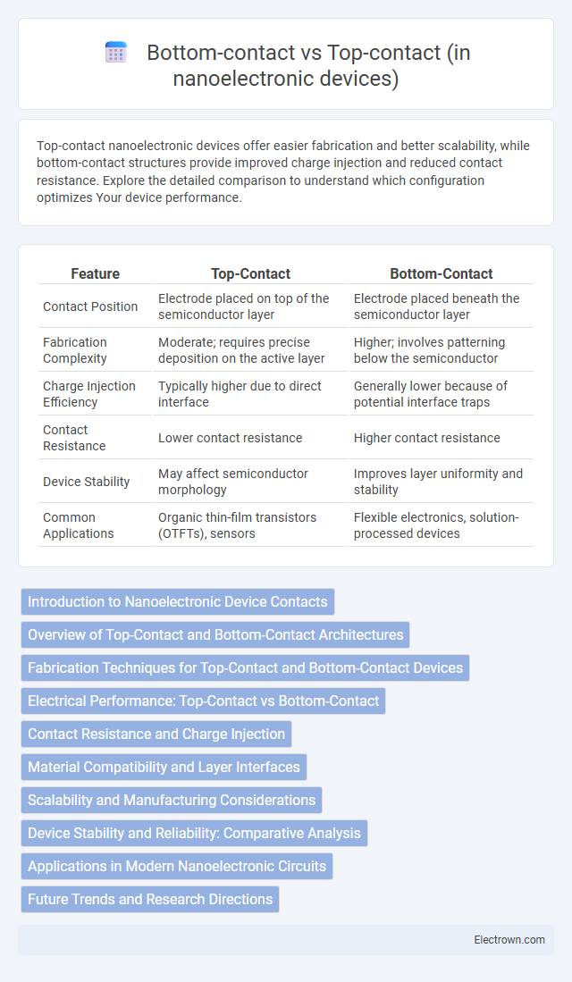
Table of Comparison
| Feature | Top-Contact | Bottom-Contact |
|---|---|---|
| Contact Position | Electrode placed on top of the semiconductor layer | Electrode placed beneath the semiconductor layer |
| Fabrication Complexity | Moderate; requires precise deposition on the active layer | Higher; involves patterning below the semiconductor |
| Charge Injection Efficiency | Typically higher due to direct interface | Generally lower because of potential interface traps |
| Contact Resistance | Lower contact resistance | Higher contact resistance |
| Device Stability | May affect semiconductor morphology | Improves layer uniformity and stability |
| Common Applications | Organic thin-film transistors (OTFTs), sensors | Flexible electronics, solution-processed devices |
Introduction to Nanoelectronic Device Contacts
Top-contact and bottom-contact configurations in nanoelectronic devices refer to the positioning of electrodes relative to the active semiconductor layer, significantly affecting charge injection and device performance. Top-contact involves electrodes placed above the semiconductor, offering better electrical contact and reduced interface resistance, whereas bottom-contact positions electrodes beneath, facilitating easier fabrication and integration with substrates. Your choice between these contact types influences device efficiency, scalability, and overall functionality in applications like organic transistors and sensors.
Overview of Top-Contact and Bottom-Contact Architectures
Top-contact and bottom-contact architectures differ in the placement of electrodes relative to the semiconductor layer in nanoelectronic devices. In top-contact devices, electrodes are deposited above the semiconductor material, offering better charge injection but potential interface damage during fabrication. Bottom-contact structures position electrodes beneath the semiconductor, providing improved contact definition and reduced damage, yet face challenges with charge injection efficiency and interface cleanliness.
Fabrication Techniques for Top-Contact and Bottom-Contact Devices
Top-contact devices typically use lithography and metal evaporation techniques to deposit electrodes directly onto the active layer, enabling precise control of contact area and resistance. Bottom-contact fabrication involves first patterning metal electrodes on the substrate followed by the deposition or growth of the semiconductor material, which demands careful alignment and surface treatment to ensure good interface quality. Both approaches rely on techniques such as photolithography, electron beam lithography, and thermal evaporation, but bottom-contact devices often require additional surface functionalization to improve semiconductor adhesion and charge injection.
Electrical Performance: Top-Contact vs Bottom-Contact
Top-contact nanoelectronic devices typically offer lower contact resistance and improved charge injection due to direct electrode deposition on the semiconductor surface, enhancing electrical performance. Bottom-contact configurations often exhibit higher contact resistance caused by poor interface quality and limited contact area, which can hinder device efficiency. Your device's electrical characteristics can significantly benefit from choosing a top-contact architecture for optimized current flow and reduced interface barriers.
Contact Resistance and Charge Injection
Top-contact nanoelectronic devices typically exhibit lower contact resistance due to improved metal-semiconductor interface quality and enhanced surface contact area that facilitates efficient charge injection. Bottom-contact configurations often suffer from higher contact resistance caused by imperfect interface formation and limited overlap between the metal electrode and the active semiconductor layer, which impedes efficient carrier injection. Optimizing contact materials and interface engineering in both approaches is crucial for minimizing charge injection barriers and enhancing overall device performance.
Material Compatibility and Layer Interfaces
Top-contact nanoelectronic devices exhibit superior material compatibility by enabling direct metal deposition on the active semiconductor layer, minimizing interface contamination and ensuring low contact resistance. Bottom-contact configurations often face challenges with layer interface quality due to the metal contacts being deposited before the semiconductor, causing poor adhesion and increased interface traps. Optimizing the interface between electrodes and semiconductor layers is crucial for enhancing charge injection efficiency and device performance in both contact schemes.
Scalability and Manufacturing Considerations
Top-contact designs in nanoelectronic devices offer easier scalability due to simplified lithography processes and better alignment control, facilitating mass production. Bottom-contact configurations pose challenges in manufacturing as the contacts must be patterned before the active layer deposition, requiring precise substrate preparation and limiting device miniaturization. Scalability in top-contact devices is enhanced by improved electrical contact and reduced parasitic resistances, making them more suitable for high-density integration in flexible electronics and large-area sensor arrays.
Device Stability and Reliability: Comparative Analysis
Top-contact nanoelectronic devices exhibit enhanced stability due to reduced metal diffusion and improved interface quality compared to bottom-contact configurations, which often suffer from higher contact resistance and interface trap density. Bottom-contact devices typically show lower long-term reliability as metal electrodes deposited beneath the active layer can induce structural defects and degrade semiconductor materials over time. Studies indicate that the superior mechanical robustness and minimized interface disruption in top-contact designs lead to improved operational lifespans and consistent electrical performance under stress conditions.
Applications in Modern Nanoelectronic Circuits
Top-contact configurations are widely used in flexible and wearable nanoelectronic devices due to their ease of fabrication and compatibility with organic semiconductors, optimizing current injection and device performance. Bottom-contact structures offer superior interface control and reduced contact resistance, making them ideal for high-frequency transistors and integrated circuits in advanced nanoelectronic applications. Your choice between top-contact and bottom-contact designs directly impacts device reliability and efficiency in cutting-edge electronic circuits.
Future Trends and Research Directions
Top-contact and bottom-contact configurations in nanoelectronic devices are evolving with innovations aimed at enhancing charge injection efficiency and device scalability. Research trends emphasize developing hybrid contact architectures and exploring novel materials like 2D semiconductors and conductive polymers to improve interface properties and minimize contact resistance. Your advancements in these areas will pave the way for more reliable, high-performance nanoscale electronics, crucial for future flexible and wearable technologies.
Top-contact vs Bottom-contact (in nanoelectronic devices) Infographic