Quantum wells confine electrons or holes in one dimension, creating a two-dimensional electron gas that allows for efficient charge carrier movement, while quantum dots confine particles in all three dimensions, resulting in discrete energy levels similar to atoms. Understanding these differences is crucial for tailoring optoelectronic devices and can help you determine which nanostructure best suits your application--explore the full article to learn more.
Table of Comparison
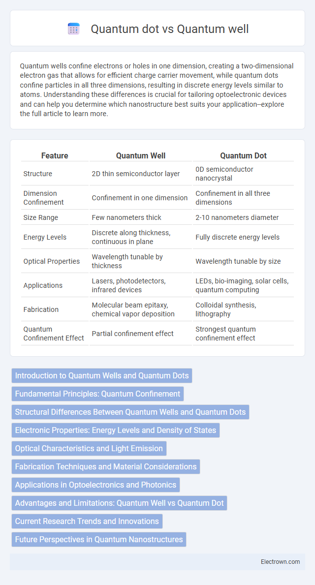
| Feature | Quantum Well | Quantum Dot |
|---|---|---|
| Structure | 2D thin semiconductor layer | 0D semiconductor nanocrystal |
| Dimension Confinement | Confinement in one dimension | Confinement in all three dimensions |
| Size Range | Few nanometers thick | 2-10 nanometers diameter |
| Energy Levels | Discrete along thickness, continuous in plane | Fully discrete energy levels |
| Optical Properties | Wavelength tunable by thickness | Wavelength tunable by size |
| Applications | Lasers, photodetectors, infrared devices | LEDs, bio-imaging, solar cells, quantum computing |
| Fabrication | Molecular beam epitaxy, chemical vapor deposition | Colloidal synthesis, lithography |
| Quantum Confinement Effect | Partial confinement effect | Strongest quantum confinement effect |
Introduction to Quantum Wells and Quantum Dots
Quantum wells are semiconductor structures where charge carriers are confined in one dimension, creating a thin layer that restricts electron movement and enhances optical and electronic properties. Quantum dots, on the other hand, confine electrons in all three spatial dimensions, forming nanoscale particles with discrete energy levels and size-tunable emission spectra. Both structures are fundamental in nanotechnology and optoelectronics, enabling advanced applications in lasers, photodetectors, and quantum computing due to their unique quantum confinement effects.
Fundamental Principles: Quantum Confinement
Quantum wells restrict electron motion in one dimension, creating a two-dimensional electron gas that enhances energy quantization and alters electronic properties. Quantum dots confine electrons in all three spatial dimensions, resulting in zero-dimensional systems with discrete energy levels similar to atoms. This quantum confinement effect in quantum dots leads to size-dependent optical and electronic characteristics, unlike quantum wells which exhibit continuous subbands.
Structural Differences Between Quantum Wells and Quantum Dots
Quantum wells are two-dimensional semiconductor structures where charge carriers are confined in one dimension, typically formed by sandwiching a thin layer of a lower bandgap material between layers of higher bandgap materials. Quantum dots, in contrast, are zero-dimensional nanostructures with quantum confinement in all three spatial dimensions, resulting in discrete energy levels similar to atoms. The structural difference stems from dimensionality: quantum wells have planar confinement, whereas quantum dots possess a confined volume, leading to distinct optical and electronic properties.
Electronic Properties: Energy Levels and Density of States
Quantum wells exhibit discrete energy levels with a continuous density of states in two dimensions, allowing electrons to move freely within the plane but confining them vertically. Quantum dots possess fully discrete energy levels and a zero-dimensional density of states, resulting in atom-like behavior with quantized energy states in all spatial directions. These differences impact their electronic properties, influencing applications in optoelectronics and quantum computing.
Optical Characteristics and Light Emission
Quantum wells confine electrons and holes in a two-dimensional plane, resulting in discrete energy levels that enhance optical gain and produce narrow emission spectra ideal for lasers and LEDs. Quantum dots, with three-dimensional electron confinement, exhibit size-tunable emission wavelengths and higher photoluminescence efficiency due to reduced non-radiative recombination. Your choice between quantum wells and quantum dots influences device performance, particularly in terms of emission wavelength control and spectral purity.
Fabrication Techniques and Material Considerations
Quantum wells are typically fabricated using epitaxial growth methods such as molecular beam epitaxy (MBE) or metal-organic chemical vapor deposition (MOCVD) to create thin, planar semiconductor layers with precise thickness control. Quantum dots are often produced using self-assembly techniques or colloidal synthesis, enabling three-dimensional confinement by forming nanoscale semiconductor particles. Material considerations for quantum wells focus on lattice-matched semiconductor pairs like GaAs/AlGaAs, whereas quantum dots require materials with suitable bandgap properties and surface passivation to prevent non-radiative recombination, ensuring your device performance meets desired specifications.
Applications in Optoelectronics and Photonics
Quantum wells are extensively used in lasers and photodetectors due to their tunable electronic and optical properties, enabling efficient light emission and detection in devices like semiconductor lasers and modulators. Quantum dots offer size-dependent emission wavelengths and high quantum efficiency, making them ideal for applications in quantum dot LEDs, display technologies, and bio-imaging photonics. Both nanostructures enhance device performance by providing strong carrier confinement, crucial for advancing optoelectronic and photonic technologies.
Advantages and Limitations: Quantum Well vs Quantum Dot
Quantum wells offer well-defined energy states and are easier to fabricate with current semiconductor technologies, making them advantageous for applications like laser diodes and photodetectors due to their high electron mobility and efficient carrier confinement. Quantum dots provide superior quantum confinement in all three spatial dimensions, enabling discrete energy levels and size-tunable optical properties, which are highly valuable for applications in quantum computing, bio-imaging, and solar cells. Limitations of quantum wells include limited quantum confinement in only one dimension and potential carrier leakage, while quantum dots face challenges in scalable manufacturing, uniformity control, and integration into existing electronic devices.
Current Research Trends and Innovations
Current research trends in quantum wells focus on enhancing electron mobility and tunable wavelength emissions for high-performance optoelectronic devices, while quantum dot studies emphasize size-dependent quantum confinement effects for applications in quantum computing and bioimaging. Innovations in quantum well technology involve integrating two-dimensional materials to improve carrier confinement and interface quality, whereas quantum dot advancements include developing hybrid perovskite quantum dots with superior photostability and multifunctionality. Both structures are central to next-generation photonic and electronic devices, with ongoing work targeting improved efficiency, scalability, and environmental stability.
Future Perspectives in Quantum Nanostructures
Quantum wells provide two-dimensional electron confinement enabling high-speed electronic and optoelectronic devices, while quantum dots offer zero-dimensional confinement with discrete energy levels ideal for quantum computing and advanced photonics. Future perspectives in quantum nanostructures emphasize hybrid systems integrating quantum wells and dots to enhance tunability, coherence, and scalability in quantum communication and sensing technologies. Emerging materials like perovskites and two-dimensional semiconductors are expected to further revolutionize these nanostructures, fostering breakthroughs in energy-efficient quantum devices.
Quantum well vs Quantum dot Infographic