Stacked Nanosheet FETs offer enhanced scalability and better electrostatic control by vertically stacking multiple nanosheets, while Gate-All-Around (GAA) FETs provide excellent channel control by surrounding the channel with gate material on all sides. Explore the article to understand how these transistor architectures impact your device performance and future semiconductor technologies.
Table of Comparison
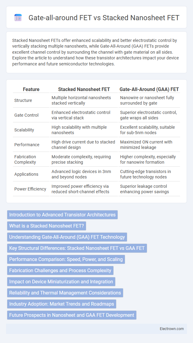
| Feature | Stacked Nanosheet FET | Gate-All-Around (GAA) FET |
|---|---|---|
| Structure | Multiple horizontal nanosheets stacked vertically | Nanowire or nanosheet fully surrounded by gate |
| Gate Control | Enhanced electrostatic control via vertical stack | Superior electrostatic control, gate wraps all sides |
| Scalability | High scalability with multiple nanosheets | Excellent scalability, suitable for sub-5nm nodes |
| Performance | High drive current due to stacked channel design | Maximized ON current with minimized leakage |
| Fabrication Complexity | Moderate complexity, requiring precise stacking | Higher complexity, especially for nanowire formation |
| Applications | Advanced logic devices in 3nm and beyond nodes | Cutting-edge transistors in future technology nodes |
| Power Efficiency | Improved power efficiency via reduced short-channel effects | Superior leakage control enhancing power savings |
Introduction to Advanced Transistor Architectures
Stacked Nanosheet FETs and Gate-All-Around (GAA) FETs represent advanced transistor architectures designed to overcome short-channel effects in nanoscale semiconductor devices. Stacked Nanosheet FETs feature multiple horizontal nanosheets vertically stacked to enhance drive current and improve electrostatic control, while GAA FETs envelop the channel with the gate material, providing superior gate electrostatics and reduced leakage. These architectures are crucial for scaling beyond FinFET technology, enabling higher performance and energy efficiency in cutting-edge integrated circuits.
What is a Stacked Nanosheet FET?
A Stacked Nanosheet FET is an advanced transistor architecture that utilizes multiple nanosheet channels stacked vertically to enhance current drive and improve electrostatic control. Each nanosheet acts as an independent channel controlled simultaneously by a gate-all-around configuration, optimizing device scaling and performance in semiconductor technology nodes beyond 5nm. This design enables better short-channel effects suppression compared to traditional Gate-all-around FETs by increasing effective channel width while maintaining a compact footprint.
Understanding Gate-All-Around (GAA) FET Technology
Gate-All-Around (GAA) FET technology offers superior electrostatic control by surrounding the channel with the gate on all sides, minimizing short-channel effects and improving device scalability compared to traditional FinFETs. Stacked Nanosheet FETs, a type of GAA device, utilize multiple thin semiconductor sheets vertically stacked to increase drive current while maintaining excellent gate control, enabling enhanced performance in advanced node transistors such as 3nm technology. The transition to GAA architectures like stacked nanosheets supports continued Moore's Law scaling by improving power efficiency, drive current, and reducing leakage current in nanoscale semiconductor devices.
Key Structural Differences: Stacked Nanosheet FET vs GAA FET
Stacked Nanosheet FETs feature multiple horizontal nanosheets vertically stacked and independently controlled, enabling enhanced gate electrostatic control and improved drive current compared to traditional Gate-All-Around (GAA) FETs. In contrast, GAA FETs typically utilize a single nanowire or nanosheet fully surrounded by the gate, providing superior gate control but less scalability in drive current. The multi-layer stacking in Stacked Nanosheet FETs allows for greater transistor density and improved performance in advanced semiconductor nodes.
Performance Comparison: Speed, Power, and Scaling
Stacked nanosheet FETs exhibit enhanced electrostatic control and higher drive current compared to gate-all-around (GAA) FETs, enabling faster switching speeds and improved device performance. Power efficiency in stacked nanosheet FETs is optimized through reduced leakage currents and lower operating voltages, contributing to superior energy savings versus traditional GAA architectures. In terms of scaling, stacked nanosheet FETs support more aggressive channel width scaling and better short-channel effect suppression, making them more suitable for advanced technology nodes below 3nm.
Fabrication Challenges and Process Complexity
Stacked Nanosheet FETs present significant fabrication challenges due to the precise layer stacking and thickness control required for optimal performance, demanding advanced lithography and etching techniques. Gate-all-around (GAA) FETs involve complex three-dimensional gate wrapping that necessitates intricate fabrication steps, including sacrificial layer removal and conformal deposition, increasing process complexity. Your choice between these technologies should consider the trade-offs in manufacturing scalability and yield impacted by these fabrication intricacies.
Impact on Device Miniaturization and Integration
Stacked Nanosheet FETs enable superior device miniaturization by offering enhanced gate control through multiple vertically stacked channels, improving electrostatic integrity compared to Gate-all-around (GAA) FETs which surround a single channel. The architecture of Stacked Nanosheet FETs supports higher drive current density and scaling efficiency, facilitating greater transistor density and integration on advanced semiconductor nodes below 3nm. This leads to significant improvements in power efficiency and overall chip performance, critical for next-generation high-performance computing and mobile applications.
Reliability and Thermal Management Considerations
Stacked Nanosheet FETs offer enhanced reliability due to their robust electrostatic control and reduced short-channel effects compared to Gate-All-Around (GAA) FETs, which face more pronounced variability challenges under high bias conditions. Thermal management is more efficient in Stacked Nanosheet FETs since their three-dimensional channel architecture facilitates better heat dissipation across multiple nanosheets, reducing localized hot spots prevalent in conventional GAA FET designs. Optimizing your device's performance involves balancing these reliability benefits with the improved thermal conductivity inherent to Stacked Nanosheet configurations for advanced semiconductor applications.
Industry Adoption: Market Trends and Roadmaps
Stacked Nanosheet FETs are gaining traction in the semiconductor industry due to their superior scalability and performance improvements over traditional Gate-All-Around (GAA) FETs, making them a focal point in advanced node roadmaps by leading foundries like TSMC and Samsung. Market trends indicate a shift towards Stacked Nanosheet architectures in the 3nm and beyond technology nodes, driven by the demand for higher transistor density and better power efficiency in mobile and high-performance computing applications. Your design strategy can benefit from aligning with this industry adoption trend, as major chipmakers integrate Stacked Nanosheet FETs into their production pipelines to meet future performance and scaling challenges.
Future Prospects in Nanosheet and GAA FET Development
Stacked Nanosheet FETs offer enhanced scalability and drive current by vertically stacking multiple nanosheets, improving transistor performance as device dimensions shrink. Gate-All-Around (GAA) FETs provide superior electrostatic control, reducing short-channel effects and enabling further miniaturization beyond FinFET technology. Your semiconductor designs will benefit from ongoing advances in both architectures, driving innovation in energy efficiency and computational power for future technology nodes.
Stacked Nanosheet FET vs Gate-all-around FET Infographic