Top-gate FETs offer superior electrostatic control and reduced short-channel effects due to their closer gate-channel proximity, while bottom-gate FETs benefit from simpler fabrication processes and better compatibility with certain substrates. Understanding these key differences can help you select the ideal transistor architecture for your specific application needs--read on to explore their detailed advantages and use cases.
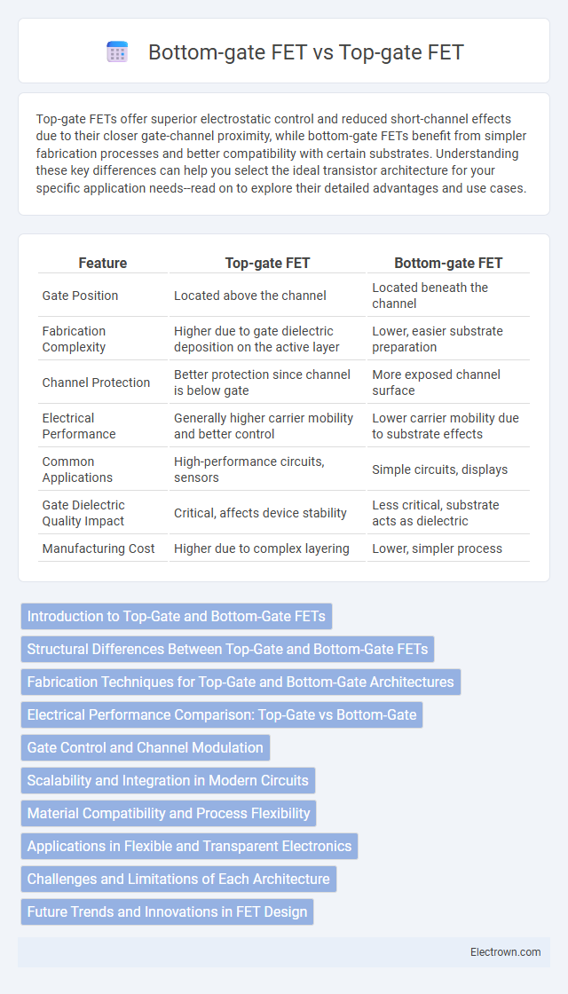
Table of Comparison
| Feature | Top-gate FET | Bottom-gate FET |
|---|---|---|
| Gate Position | Located above the channel | Located beneath the channel |
| Fabrication Complexity | Higher due to gate dielectric deposition on the active layer | Lower, easier substrate preparation |
| Channel Protection | Better protection since channel is below gate | More exposed channel surface |
| Electrical Performance | Generally higher carrier mobility and better control | Lower carrier mobility due to substrate effects |
| Common Applications | High-performance circuits, sensors | Simple circuits, displays |
| Gate Dielectric Quality Impact | Critical, affects device stability | Less critical, substrate acts as dielectric |
| Manufacturing Cost | Higher due to complex layering | Lower, simpler process |
Introduction to Top-Gate and Bottom-Gate FETs
Top-gate FETs feature the gate electrode positioned above the semiconductor channel, enabling better electrostatic control and reduced short-channel effects, making them ideal for high-performance applications. Bottom-gate FETs, with the gate electrode beneath the semiconductor layer, offer simpler fabrication and improved stability, commonly used in thin-film transistors and flexible electronics. The choice between top-gate and bottom-gate architectures depends on factors like device performance, manufacturing complexity, and intended application domain.
Structural Differences Between Top-Gate and Bottom-Gate FETs
Top-gate FETs feature a gate electrode positioned above the semiconductor channel, separated by a dielectric layer, which allows for better gate control and reduced parasitic capacitance. Bottom-gate FETs have the gate electrode located beneath the semiconductor layer, often integrated on the substrate, leading to simpler fabrication but potential challenges in gate-channel alignment and increased interface traps. Your choice between these structures impacts device performance, fabrication complexity, and integration suitability in electronic applications.
Fabrication Techniques for Top-Gate and Bottom-Gate Architectures
Top-gate FETs are typically fabricated using a sequence where the gate dielectric and electrode are deposited above the semiconductor layer, allowing for improved interface quality and enhanced device scalability. Bottom-gate FET fabrication involves patterning the gate electrode first on the substrate, followed by the deposition of the gate dielectric and semiconductor layer, which simplifies alignment and is compatible with large-area processing. Advanced techniques such as atomic layer deposition (ALD) for dielectrics and inkjet printing for semiconductors are frequently employed to optimize performance in both architectures.
Electrical Performance Comparison: Top-Gate vs Bottom-Gate
Top-gate FETs exhibit superior electrical performance due to enhanced gate control and reduced parasitic capacitance, resulting in higher carrier mobility and improved on/off current ratios compared to bottom-gate FETs. Bottom-gate FETs often suffer from degraded channel quality caused by dielectric-semiconductor interface traps, leading to lower threshold voltage stability and increased subthreshold slope. Consequently, top-gate FET architectures are preferred for high-frequency and low-power applications demanding precise electrostatic control and robust performance metrics.
Gate Control and Channel Modulation
Top-gate FETs offer superior gate control due to the gate electrode's proximity to the semiconductor channel, enabling stronger electric field modulation and enhanced channel conductivity. Bottom-gate FETs exhibit weaker gate control since the gate lies beneath the substrate, which increases the gate-to-channel distance and reduces electrostatic coupling. Channel modulation in top-gate devices benefits from reduced scattering and improved carrier mobility, while bottom-gate devices often face increased parasitic capacitances, limiting switching speed and overall device performance.
Scalability and Integration in Modern Circuits
Top-gate FETs offer superior scalability due to their reduced parasitic capacitance and better electrostatic control, making them ideal for high-density integration in modern circuits. Bottom-gate FETs, while simpler to fabricate, often face limitations in scaling because of increased leakage currents and less effective gate control. Your choice between the two should consider the trade-offs in device performance and integration complexity for next-generation semiconductor technologies.
Material Compatibility and Process Flexibility
Top-gate FETs offer superior material compatibility by allowing diverse semiconductor and dielectric materials to be deposited beneath the gate electrode, enabling enhanced interface quality and device performance. Bottom-gate FETs provide greater process flexibility due to their simpler fabrication steps, as the gate electrode is pre-patterned on the substrate, facilitating easy integration with various substrates and scalable manufacturing. Both architectures impact the choice of materials and processes, influencing device stability, threshold voltage control, and overall circuit design considerations.
Applications in Flexible and Transparent Electronics
Top-gate FETs offer superior control over the channel, making them ideal for high-performance flexible and transparent electronics such as wearable sensors and flexible displays. Bottom-gate FETs provide simpler fabrication and better substrate compatibility, which suits applications like large-area flexible circuits and low-cost organic electronics. Both structures enable advancements in transparent oxide semiconductors and polymer-based flexible devices, optimizing device stability and mechanical flexibility.
Challenges and Limitations of Each Architecture
Top-gate FETs often face challenges such as complex fabrication processes and difficulty in achieving uniform gate dielectric layers, which can limit device performance and reliability. Bottom-gate FETs typically suffer from poor channel control and increased short-channel effects due to the distance between the gate electrode and the channel, leading to lower device efficiency. Understanding these constraints helps you select the optimal FET architecture based on your specific application requirements and performance criteria.
Future Trends and Innovations in FET Design
Top-gate FETs are gaining traction in flexible electronics due to their superior channel protection and enhanced electrostatic control, which fosters innovations in transparent and wearable devices. Bottom-gate FETs remain prominent for large-area applications, benefiting from simplified fabrication and compatibility with existing silicon technology, driving cost-effective solutions. Your choice between these architectures will increasingly depend on the specific requirements for device flexibility, scalability, and performance in next-generation electronic systems.
Top-gate FET vs Bottom-gate FET Infographic