Direct-write lithography offers unparalleled flexibility and precision by directly patterning substrates without the need for masks, reducing costs and enabling rapid prototyping. Explore the rest of the article to discover how your choice between direct-write and mask-based lithography impacts fabrication efficiency and design complexity.
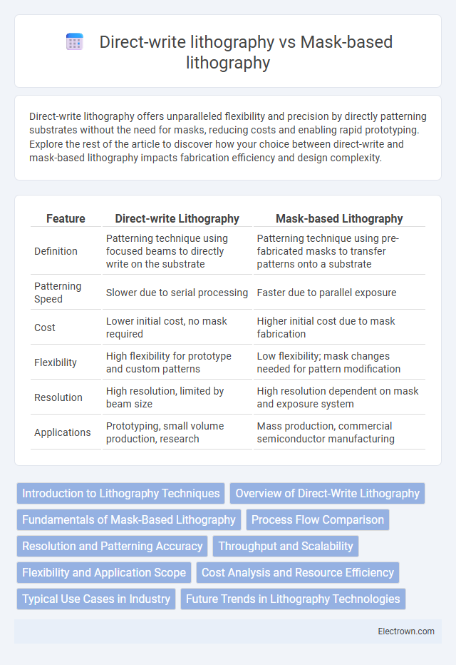
Table of Comparison
| Feature | Direct-write Lithography | Mask-based Lithography |
|---|---|---|
| Definition | Patterning technique using focused beams to directly write on the substrate | Patterning technique using pre-fabricated masks to transfer patterns onto a substrate |
| Patterning Speed | Slower due to serial processing | Faster due to parallel exposure |
| Cost | Lower initial cost, no mask required | Higher initial cost due to mask fabrication |
| Flexibility | High flexibility for prototype and custom patterns | Low flexibility; mask changes needed for pattern modification |
| Resolution | High resolution, limited by beam size | High resolution dependent on mask and exposure system |
| Applications | Prototyping, small volume production, research | Mass production, commercial semiconductor manufacturing |
Introduction to Lithography Techniques
Direct-write lithography employs focused beams such as electron or ion beams to pattern substrates without using masks, enabling high-resolution and flexible patterning for prototyping and low-volume production. Mask-based lithography utilizes photomasks to transfer patterns onto photosensitive materials, offering high throughput suitable for mass production in semiconductor manufacturing. Both techniques serve critical roles in microfabrication, with direct-write lithography favoring precision and customization, while mask-based lithography emphasizes speed and cost-efficiency in large-scale manufacturing.
Overview of Direct-Write Lithography
Direct-write lithography is a maskless patterning technique that uses focused beams, such as electrons or ions, to directly write patterns onto a substrate, enabling high-resolution and flexible fabrication. Unlike mask-based lithography, it eliminates the need for photomasks, reducing setup time and costs for low-volume or prototype production. This method supports rapid iteration and customization, making it ideal for research and development in microelectronics and nanotechnology.
Fundamentals of Mask-Based Lithography
Mask-based lithography relies on photomasks to project intricate circuit patterns onto semiconductor wafers using ultraviolet light, enabling rapid and precise replication of micro-scale features. This technique leverages intricate optics systems, such as stepper and scanner machines, to achieve high throughput and consistent pattern fidelity across large wafer surfaces. The process efficiency stems from its ability to simultaneously expose entire wafer areas through the mask, making it a cornerstone technology for mass semiconductor manufacturing.
Process Flow Comparison
Direct-write lithography skips the creation of photomasks, enabling faster prototyping by directly patterning the substrate with a focused beam, whereas mask-based lithography involves complex mask fabrication followed by exposure and development steps. The mask-based process provides high throughput and uniformity for volume production, relying on photomasks to transfer patterns across the wafer. Your choice depends on the trade-off between flexibility and speed in direct-write methods versus the efficiency and repeatability of mask-based lithography.
Resolution and Patterning Accuracy
Direct-write lithography achieves superior resolution and patterning accuracy by using focused beams or probes to directly inscribe patterns without masks, enabling feature sizes down to the nanometer scale. Mask-based lithography relies on photomasks for pattern transfer, which can introduce distortions and limit resolution due to mask defects and optical proximity effects. Your choice depends on whether ultimate precision or high-throughput patterning is prioritized, as direct-write excels in accuracy but is slower, while mask-based lithography offers faster production with moderate resolution.
Throughput and Scalability
Direct-write lithography offers high flexibility and precision for small-scale and custom patterning but suffers from limited throughput due to its serial writing process, making it less scalable for mass production. Mask-based lithography excels in throughput and scalability by enabling parallel pattern transfer across entire wafers, significantly accelerating manufacturing speeds and reducing per-unit costs. Your choice hinges on balancing the need for rapid, large-volume fabrication with the demand for intricate or variable design features.
Flexibility and Application Scope
Direct-write lithography offers superior flexibility by enabling maskless patterning, allowing rapid prototyping and customization for diverse applications, including complex and low-volume designs. Mask-based lithography excels in high-volume, repeatable manufacturing due to its reliance on pre-fabricated masks, making it ideal for mass production of integrated circuits and standardized components. Your choice depends on whether you prioritize adaptable, cost-effective development or high-throughput, consistent fabrication processes.
Cost Analysis and Resource Efficiency
Direct-write lithography offers lower initial capital investment compared to mask-based lithography, eliminating the need for expensive photomasks and reducing upfront costs significantly. Mask-based lithography achieves higher throughput and is more resource-efficient for large-scale production due to batch processing, lowering per-unit cost over time despite high initial expenses. In summary, direct-write lithography is cost-effective for prototyping and low-volume manufacturing, while mask-based lithography provides better resource efficiency and cost advantages in mass production scenarios.
Typical Use Cases in Industry
Direct-write lithography is predominantly used in prototyping, custom microfabrication, and low-volume production due to its maskless operation and high flexibility for design changes. Mask-based lithography, such as photolithography, dominates high-volume semiconductor manufacturing where consistent replication of intricate patterns on silicon wafers is critical. Industries that require rapid iteration or niche applications, like MEMS devices and PCB fabrication, prefer direct-write methods, while large-scale integrated circuit (IC) fabrication relies heavily on mask-based lithography for efficiency and cost-effectiveness.
Future Trends in Lithography Technologies
Direct-write lithography offers unparalleled flexibility for prototyping and customized patterns by eliminating the need for masks, making it increasingly valuable in rapid microfabrication and research environments. Mask-based lithography remains dominant in large-scale semiconductor manufacturing due to its high throughput and precision, but evolving techniques like extreme ultraviolet (EUV) lithography are pushing its resolution limits further. Your choice between these technologies will likely depend on balancing speed, cost, and complexity as future trends favor hybrid approaches integrating direct-write methods for niche applications alongside advanced mask-based systems.
Direct-write lithography vs Mask-based lithography Infographic