STM lithography offers atomic-scale precision by manipulating individual atoms using a scanning tunneling microscope, ideal for creating ultra-fine nanostructures on conductive surfaces. AFM lithography, utilizing an atomic force microscope, provides versatile patterning on a wider range of materials, including insulators, through mechanical, thermal, or electrical modifications; explore the article to understand which method best suits your nanofabrication needs.
Table of Comparison
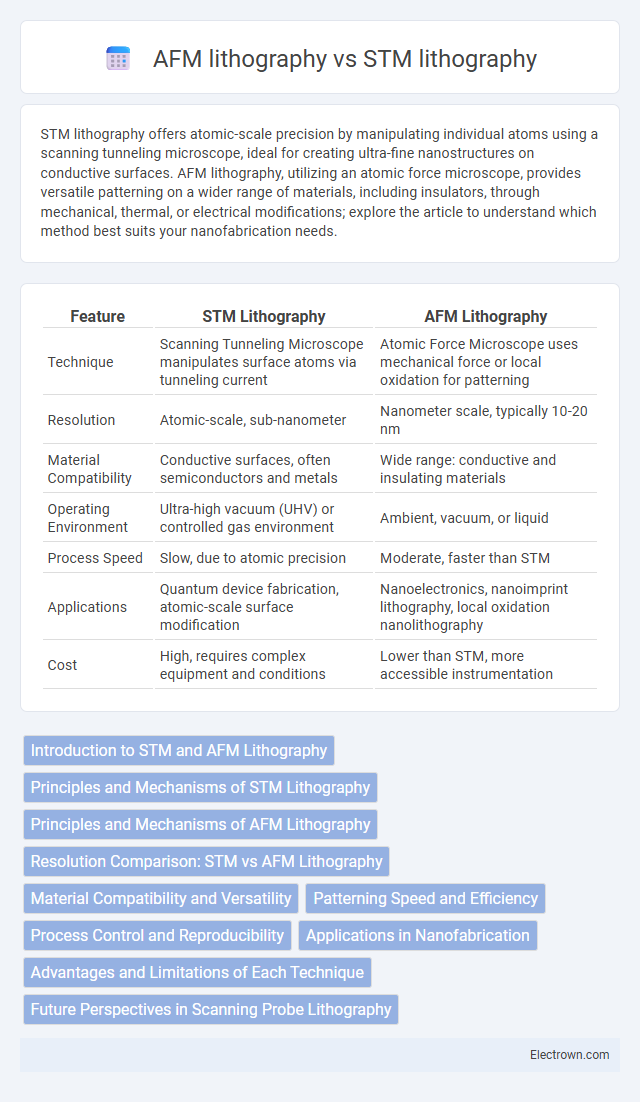
| Feature | STM Lithography | AFM Lithography |
|---|---|---|
| Technique | Scanning Tunneling Microscope manipulates surface atoms via tunneling current | Atomic Force Microscope uses mechanical force or local oxidation for patterning |
| Resolution | Atomic-scale, sub-nanometer | Nanometer scale, typically 10-20 nm |
| Material Compatibility | Conductive surfaces, often semiconductors and metals | Wide range: conductive and insulating materials |
| Operating Environment | Ultra-high vacuum (UHV) or controlled gas environment | Ambient, vacuum, or liquid |
| Process Speed | Slow, due to atomic precision | Moderate, faster than STM |
| Applications | Quantum device fabrication, atomic-scale surface modification | Nanoelectronics, nanoimprint lithography, local oxidation nanolithography |
| Cost | High, requires complex equipment and conditions | Lower than STM, more accessible instrumentation |
Introduction to STM and AFM Lithography
Scanning Tunneling Microscopy (STM) lithography utilizes the quantum tunneling effect to manipulate surfaces at the atomic scale, enabling precise patterning on conductive materials with sub-nanometer resolution. Atomic Force Microscopy (AFM) lithography employs a sharp cantilever tip to physically or chemically modify the surface of various substrates, offering versatility across conductive and insulating materials with nanometer-scale accuracy. Both techniques are pivotal in nanofabrication, with STM excelling in atomic precision on conductive surfaces, while AFM provides broader material compatibility and diverse patterning methods.
Principles and Mechanisms of STM Lithography
STM lithography operates by exploiting the tunneling current between a sharp conductive tip and a conductive surface to induce localized chemical reactions or physical changes at the atomic scale. The mechanism involves precise electron tunneling that can remove or modify surface atoms, enabling high-resolution patterning with atomic precision. Your control over the tip's position and applied voltage allows for the creation of nanoscale structures, distinguishing STM lithography by its capability for direct-write fabrication without resist materials.
Principles and Mechanisms of AFM Lithography
AFM lithography operates by using an atomic force microscope's sharp tip to mechanically or chemically alter surfaces at the nanoscale, creating precise patterns through direct interaction. Unlike STM lithography, which relies on tunneling current to manipulate surface atoms, AFM lithography utilizes physical forces such as indentation, local oxidation, or dip-pen nanolithography to achieve high-resolution patterning. Your ability to control these mechanisms enables versatile applications in nanofabrication, especially on insulating substrates.
Resolution Comparison: STM vs AFM Lithography
Scanning Tunneling Microscopy (STM) lithography offers superior resolution, achieving atomic-scale precision due to its ability to manipulate individual atoms through electron tunneling. Atomic Force Microscopy (AFM) lithography provides lower spatial resolution, typically in the range of a few nanometers, as it relies on mechanical interaction between the probe tip and the surface. STM's resolution commonly reaches sub-nanometer levels, outperforming AFM in applications requiring atomic-level patterning and manipulation.
Material Compatibility and Versatility
STM lithography excels in patterning conductive and semiconductive materials due to its reliance on tunneling current, making it ideal for graphene, silicon, and metal surfaces. AFM lithography offers broader material compatibility, including insulators, polymers, and biological samples, thanks to its mechanical and electrochemical modification capabilities. Your choice depends on the substrate type and application requirements, with AFM providing greater versatility across diverse materials.
Patterning Speed and Efficiency
STM lithography offers higher patterning speed due to its ability to manipulate atoms with precise voltage pulses, making it suitable for creating detailed nanostructures quickly. AFM lithography, while slower, provides enhanced control over tip-surface interactions, allowing for more complex and diverse patterning techniques. Your choice depends on whether you prioritize rapid fabrication or intricate patterning capabilities.
Process Control and Reproducibility
STM lithography offers atomic-level precision by controlling electron tunneling currents, resulting in highly reproducible nanostructures essential for semiconductor device fabrication. AFM lithography relies on mechanical tip-sample interaction forces or local anodic oxidation, which can introduce variability in feature size and shape due to tip wear and environmental factors. Process control in STM lithography is enhanced by stable scanning tunneling conditions, while AFM lithography demands frequent calibration and tip replacement to maintain consistency.
Applications in Nanofabrication
STM lithography excels in creating atomic-scale patterns essential for quantum computing components and semiconductor device prototypes, offering unparalleled precision in nanoscale manipulation. AFM lithography is widely used for fabricating nanodevices like sensors and nanoscale transistors, leveraging its ability to pattern various materials through mechanical or electrochemical means. Your choice between STM and AFM lithography should consider the required resolution and material compatibility for specific nanofabrication applications.
Advantages and Limitations of Each Technique
STM lithography offers atomic-scale precision and is ideal for fabricating ultra-small devices with high spatial resolution, but it requires ultra-high vacuum and low temperatures, limiting its practical applications. AFM lithography operates under ambient conditions and allows versatile patterning on various materials, yet its spatial resolution is generally lower than STM, and tip wear can affect reproducibility. Both methods face trade-offs between resolution, environmental requirements, and throughput, influencing their suitability for specific nanofabrication tasks.
Future Perspectives in Scanning Probe Lithography
Scanning probe lithography (SPL) technologies, such as STM and AFM lithography, are evolving rapidly to enable atomic-scale patterning with unprecedented precision. STM lithography offers superior resolution by leveraging quantum tunneling to manipulate individual atoms, making it ideal for fabricating next-generation quantum devices. AFM lithography provides versatile material compatibility and three-dimensional structuring capabilities, positioning it as a key method for scalable nanomanufacturing and future integration in heterogeneous nanosystems.
STM lithography vs AFM lithography Infographic