Hybrid nanodevices combine diverse materials and components to optimize performance and functionality, while monolithic nanodevices rely on a single material system for uniformity and simplicity. Explore the detailed advantages and applications of each technology to understand which one suits Your needs best.
Table of Comparison
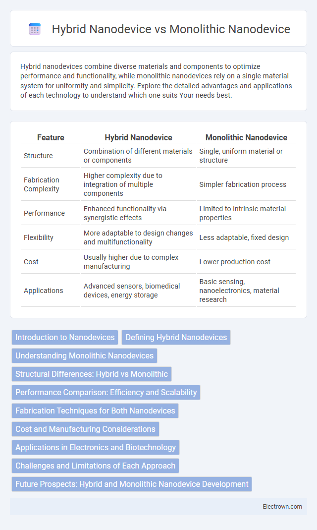
| Feature | Hybrid Nanodevice | Monolithic Nanodevice |
|---|---|---|
| Structure | Combination of different materials or components | Single, uniform material or structure |
| Fabrication Complexity | Higher complexity due to integration of multiple components | Simpler fabrication process |
| Performance | Enhanced functionality via synergistic effects | Limited to intrinsic material properties |
| Flexibility | More adaptable to design changes and multifunctionality | Less adaptable, fixed design |
| Cost | Usually higher due to complex manufacturing | Lower production cost |
| Applications | Advanced sensors, biomedical devices, energy storage | Basic sensing, nanoelectronics, material research |
Introduction to Nanodevices
Nanodevices, critical components in nanoscale technology, are engineered to perform functions at the atomic or molecular scale, enabling applications in electronics, medicine, and energy. Hybrid nanodevices integrate diverse materials or components, combining the advantages of each to enhance functionality and performance. In contrast, monolithic nanodevices consist of a single material or structure, offering uniformity and often simpler fabrication processes but with potential limitations in multifunctionality.
Defining Hybrid Nanodevices
Hybrid nanodevices integrate multiple materials or functional components at the nanoscale to enhance performance, versatility, and functionality compared to monolithic nanodevices, which rely on a single material substrate. These devices combine distinct nanoscale properties, such as semiconducting, metallic, or biological elements, enabling advanced applications in sensing, energy storage, and nanoelectronics. Understanding hybrid nanodevices helps you leverage their unique capabilities for cutting-edge technological innovations.
Understanding Monolithic Nanodevices
Monolithic nanodevices are integrated systems fabricated from a single material or substrate, offering enhanced structural uniformity and reduced interfacial defects compared to hybrid counterparts. Their monolithic architecture enables superior electrical and thermal conductivity, critical for nanoelectronics and photonics applications. Precise control over material composition and geometry at the nanoscale ensures improved device reliability and performance consistency.
Structural Differences: Hybrid vs Monolithic
Hybrid nanodevices integrate multiple distinct nanoscale materials or components, often combining organic and inorganic elements to achieve multifunctionality, whereas monolithic nanodevices are fabricated from a single, continuous material with uniform properties throughout. The structural complexity of hybrid nanodevices allows tailored interfaces and layered architectures, enhancing device performance and flexibility. Monolithic nanodevices benefit from intrinsic material uniformity, which often results in superior mechanical stability and simpler fabrication processes.
Performance Comparison: Efficiency and Scalability
Hybrid nanodevices offer superior efficiency by combining diverse materials and functions, enabling enhanced performance in energy conversion, sensing, and data processing compared to monolithic nanodevices. Scalability favors hybrid designs because their modular structure allows easier integration and customization across various applications, whereas monolithic nanodevices face limitations due to uniform material constraints. Your choice of nanodevice should consider these factors to balance performance needs with scalable production capabilities.
Fabrication Techniques for Both Nanodevices
Hybrid nanodevices are fabricated using a combination of top-down lithography and bottom-up self-assembly methods, enabling integration of diverse materials with precise nanoscale control. Monolithic nanodevices rely primarily on uniform top-down lithographic techniques such as electron-beam lithography or photolithography on a single material substrate, ensuring structural coherence and simplicity. Understanding Your choice between hybrid and monolithic fabrication impacts device complexity, scalability, and functional versatility.
Cost and Manufacturing Considerations
Hybrid nanodevices often involve higher manufacturing costs due to the complexity of integrating multiple materials and components at the nanoscale, whereas monolithic nanodevices benefit from streamlined fabrication processes using a single material system that reduces production expenses. Your choice may impact scalability, as monolithic devices typically offer better manufacturability and cost efficiency in large-volume production. Cost optimization in nanodevice manufacturing depends on balancing the performance advantages of hybrid architectures with the simpler, more economical fabrication routes of monolithic designs.
Applications in Electronics and Biotechnology
Hybrid nanodevices combine diverse materials and nanoscale components, enabling versatile applications in electronics such as flexible sensors, high-performance transistors, and energy-efficient memory devices. In biotechnology, these devices facilitate precise drug delivery systems, advanced biosensors, and diagnostic platforms by integrating biological molecules with electronic functionalities. Monolithic nanodevices, fabricated from a single material system, offer high structural uniformity and reliability, making them ideal for stable electronic circuits and implantable biosensors with consistent performance over time.
Challenges and Limitations of Each Approach
Hybrid nanodevices face significant integration challenges due to material incompatibility and complex interface engineering, which can lead to performance degradation and reduced reliability. Monolithic nanodevices are limited by fabrication constraints that restrict design flexibility and scalability, often causing difficulties in achieving multifunctionality within a single structure. Both approaches encounter issues with reproducibility and yield, impacting their practical deployment in advanced nanoelectronics and nanophotonics applications.
Future Prospects: Hybrid and Monolithic Nanodevice Development
Hybrid nanodevices integrate multiple materials and functional components, offering enhanced flexibility and scalability for future applications in nanoelectronics and sensing technologies. Monolithic nanodevices, fabricated from a single material system, provide superior reliability and uniformity, making them ideal for high-performance computing and quantum devices. Advancements in material science and nanofabrication techniques are expected to drive the development of both hybrid and monolithic nanodevices, enabling breakthroughs in energy efficiency, miniaturization, and multifunctional capabilities.
Hybrid Nanodevice vs Monolithic Nanodevice Infographic