Schottky barrier FETs utilize metal-semiconductor junctions that enable faster switching speeds and lower power consumption compared to conventional FETs with p-n junctions, making them ideal for high-frequency applications. Discover how these differences impact your circuit design by reading the rest of the article.
Table of Comparison
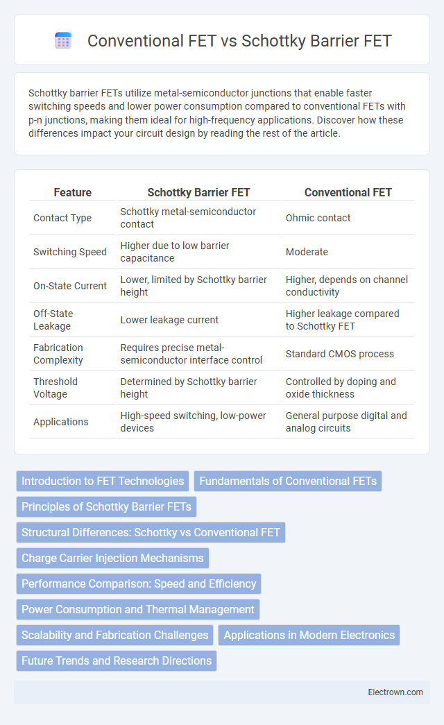
| Feature | Schottky Barrier FET | Conventional FET |
|---|---|---|
| Contact Type | Schottky metal-semiconductor contact | Ohmic contact |
| Switching Speed | Higher due to low barrier capacitance | Moderate |
| On-State Current | Lower, limited by Schottky barrier height | Higher, depends on channel conductivity |
| Off-State Leakage | Lower leakage current | Higher leakage compared to Schottky FET |
| Fabrication Complexity | Requires precise metal-semiconductor interface control | Standard CMOS process |
| Threshold Voltage | Determined by Schottky barrier height | Controlled by doping and oxide thickness |
| Applications | High-speed switching, low-power devices | General purpose digital and analog circuits |
Introduction to FET Technologies
Schottky barrier FETs utilize metal-semiconductor junctions to achieve faster switching speeds and lower power consumption compared to conventional FETs, which rely on doped semiconductor channels. The unique Schottky barrier contact reduces carrier injection delay, enhancing high-frequency performance in RF and analog applications. You can leverage Schottky barrier FET technology for improved device scaling and efficiency in advanced circuits.
Fundamentals of Conventional FETs
Conventional Field-Effect Transistors (FETs) operate based on the voltage applied to the gate terminal, which controls the conductivity of a semiconductor channel between the source and drain. The channel is typically formed in silicon, modulating current flow through electric field effects without direct injection of carriers from the gate. Your understanding of these fundamentals is essential when comparing them to Schottky barrier FETs, which utilize metal-semiconductor junctions for carrier injection.
Principles of Schottky Barrier FETs
Schottky Barrier FETs operate by utilizing a metal-semiconductor junction that forms a Schottky barrier, controlling carrier injection through tunneling effects rather than conventional charge modulation in the channel. This barrier enables faster switching speeds and lower power consumption compared to conventional FETs, which rely on impurity doping and a pn-junction to modulate current flow. Understanding your application's speed and power requirements helps determine whether a Schottky Barrier FET or a conventional FET is the optimal choice.
Structural Differences: Schottky vs Conventional FET
Schottky barrier FETs feature a metal-semiconductor junction at the source and drain, forming Schottky barriers that control carrier injection, unlike conventional FETs which use heavily doped p-n junctions for source/drain contacts. The Schottky barrier reduces the parasitic resistance and capacitance, enabling faster switching speeds and lower power consumption. Conventional FETs rely on diffusion processes during fabrication, while Schottky barrier FETs utilize metal contacts, resulting in distinct electrical characteristics and fabrication complexity.
Charge Carrier Injection Mechanisms
Schottky barrier FETs utilize metal-semiconductor junctions where charge carrier injection occurs via thermionic emission and tunneling across the Schottky barrier, resulting in potentially lower contact resistance compared to conventional FETs. Conventional FETs rely on doped semiconductor regions for carrier injection, which is primarily governed by diffusion over the built-in potential barrier. The unique injection mechanisms in Schottky barrier FETs enable faster switching speeds and better scalability for nanoscale devices.
Performance Comparison: Speed and Efficiency
Schottky barrier FETs offer faster switching speeds than conventional FETs due to lower Schottky barrier heights, which reduce carrier injection delay and enhance electron mobility. Your circuits benefit from improved efficiency since Schottky barrier FETs exhibit lower ON-resistance and reduced power consumption during operation. These performance advantages make Schottky barrier FETs well-suited for high-frequency and low-power applications compared to traditional FET technology.
Power Consumption and Thermal Management
Schottky barrier FETs exhibit lower power consumption due to their reduced contact resistance and faster switching capabilities compared to conventional FETs. Their metal-semiconductor junctions enable efficient carrier injection, minimizing energy loss and heat generation, which improves thermal management. You benefit from enhanced device reliability and longer operational lifespan in applications requiring low power and efficient heat dissipation.
Scalability and Fabrication Challenges
Schottky barrier FETs (SB-FETs) offer improved scalability over conventional FETs due to their ultrathin metal-semiconductor junctions, enabling shorter channel lengths and reduced short-channel effects. However, fabricating SB-FETs presents challenges such as precise control of the Schottky barrier height and formation of abrupt, low-resistance contacts, which are critical for device performance and reproducibility. Your choice between SB-FETs and conventional FETs depends on balancing these scalability advantages against the increased complexity and variability in manufacturing processes.
Applications in Modern Electronics
Schottky barrier FETs offer faster switching speeds and lower power consumption, making them ideal for high-frequency analog circuits and RF applications. Conventional FETs are widely used in digital logic circuits and power management due to their robust control of channel conductivity and scalability. The integration of Schottky barrier FETs in sensors and ultra-low power devices enhances performance in Internet of Things (IoT) and wearable electronics.
Future Trends and Research Directions
Schottky barrier FETs (SB-FETs) are gaining attention for their potential to overcome scaling limitations of conventional FETs by enabling ultra-short channel lengths and reduced contact resistance. Future research trends focus on material engineering of Schottky contacts and novel 2D semiconductors to enhance carrier injection and switching speed. Your exploration of device architectures integrating SB-FETs with advanced CMOS technology could drive innovations in low-power, high-frequency electronics.
Schottky barrier FET vs Conventional FET Infographic