Nanoplasmonic circuits leverage the interaction of light with metallic nanostructures to achieve ultra-fast signal processing and nanoscale integration, outperforming traditional nanoelectronic circuits in speed and bandwidth. Discover how your technology applications can benefit from these advancements by exploring the detailed comparison in the rest of this article.
Table of Comparison
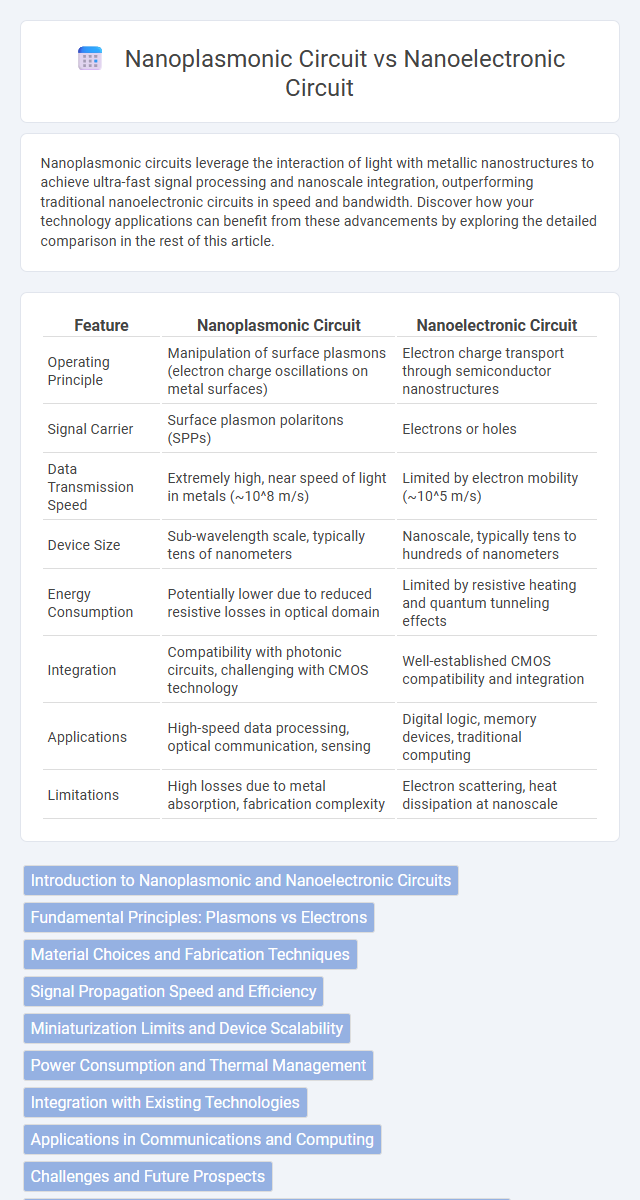
| Feature | Nanoplasmonic Circuit | Nanoelectronic Circuit |
|---|---|---|
| Operating Principle | Manipulation of surface plasmons (electron charge oscillations on metal surfaces) | Electron charge transport through semiconductor nanostructures |
| Signal Carrier | Surface plasmon polaritons (SPPs) | Electrons or holes |
| Data Transmission Speed | Extremely high, near speed of light in metals (~10^8 m/s) | Limited by electron mobility (~10^5 m/s) |
| Device Size | Sub-wavelength scale, typically tens of nanometers | Nanoscale, typically tens to hundreds of nanometers |
| Energy Consumption | Potentially lower due to reduced resistive losses in optical domain | Limited by resistive heating and quantum tunneling effects |
| Integration | Compatibility with photonic circuits, challenging with CMOS technology | Well-established CMOS compatibility and integration |
| Applications | High-speed data processing, optical communication, sensing | Digital logic, memory devices, traditional computing |
| Limitations | High losses due to metal absorption, fabrication complexity | Electron scattering, heat dissipation at nanoscale |
Introduction to Nanoplasmonic and Nanoelectronic Circuits
Nanoplasmonic circuits exploit the interaction between light and free electrons at the nanoscale to achieve ultra-fast signal processing and optical communication, surpassing traditional electronic speed limits. Nanoelectronic circuits rely on the manipulation of electrons in nanoscale semiconductor devices for data processing and storage, emphasizing miniaturization and energy efficiency. Your choice between the two technologies will depend on the specific needs for speed, integration with photonic systems, and energy consumption in advanced computing applications.
Fundamental Principles: Plasmons vs Electrons
Nanoplasmonic circuits leverage plasmons, which are collective oscillations of free electrons at the surface of metals enabling light manipulation at the nanoscale, while nanoelectronic circuits rely on the movement of individual electrons through semiconductor materials to process signals. Plasmons in nanoplasmonics provide faster data transmission speeds and enable subwavelength optical confinement beyond the diffraction limit, contrasting with electron-based nanoelectronics where slower electron mobility and heat dissipation pose challenges. Your choice between these technologies depends on whether you prioritize ultrafast optical signal processing using plasmon resonance or traditional electron charge transport in nanoscale devices.
Material Choices and Fabrication Techniques
Nanoplasmonic circuits primarily utilize noble metals such as gold and silver due to their superior plasmonic properties at optical frequencies, enabling effective light manipulation at the nanoscale. Nanoelectronic circuits often rely on semiconductor materials like silicon and gallium arsenide, fabricated through well-established processes like photolithography and chemical vapor deposition. Your choice between these circuits depends on the need for either optical signal processing with nanoplasmonics or electronic data handling with nanoelectronics, as the fabrication techniques and material compatibility vary significantly.
Signal Propagation Speed and Efficiency
Nanoplasmonic circuits leverage surface plasmons to enable signal propagation at speeds approaching the speed of light, significantly surpassing traditional nanoelectronic circuits reliant on electron flow. These circuits offer enhanced efficiency by reducing resistive losses and heat generation, which are common bottlenecks in nanoelectronic devices. Your choice between nanoplasmonic and nanoelectronic circuits should consider the trade-offs in signal speed and energy consumption for specific nanoscale applications.
Miniaturization Limits and Device Scalability
Nanoplasmonic circuits leverage surface plasmon resonances to achieve device dimensions below the diffraction limit, enabling unprecedented miniaturization compared to traditional nanoelectronic circuits constrained by electron mobility and heat dissipation. While nanoelectronic circuits face scalability challenges due to quantum tunneling and increased power density at sub-10 nm feature sizes, nanoplasmonic circuits offer enhanced scalability by manipulating light at the nanoscale, though they encounter losses from plasmonic damping. Understanding these miniaturization limits and scalability aspects allows you to optimize circuit design for next-generation high-speed, ultra-compact integrated systems.
Power Consumption and Thermal Management
Nanoplasmonic circuits exhibit significantly lower power consumption compared to nanoelectronic circuits due to their reliance on surface plasmons for signal transmission, which reduces resistive losses. Thermal management in nanoplasmonic devices is more efficient as they generate less heat and allow for localized heating control at the nanoscale. Nanoelectronic circuits, on the other hand, face challenges with heat dissipation stemming from high current densities and resistive heating, necessitating advanced cooling solutions.
Integration with Existing Technologies
Nanoplasmonic circuits integrate effectively with photonic components, enhancing data transfer speeds and enabling seamless coupling with optical fibers in telecommunications systems. Nanoelectronic circuits, based on semiconductor technology, maintain compatibility with traditional CMOS fabrication processes, facilitating integration into existing electronic devices and microchip architectures. Both approaches present unique challenges and advantages, with nanoplasmonics offering superior bandwidth and nanoelectronics providing mature manufacturing infrastructure.
Applications in Communications and Computing
Nanoplasmonic circuits leverage surface plasmon resonance to enable ultra-fast data transmission and signal processing at nanoscale dimensions, enhancing optical communication systems with higher bandwidth and lower latency compared to nanoelectronic circuits. Nanoelectronic circuits, utilizing electron charge for data manipulation, excel in traditional computing applications but face speed and heat dissipation limitations at extremely small scales. Your choice between them depends on whether high-speed optical communication or reliable electronic computing integration is the priority for your application.
Challenges and Future Prospects
Nanoplasmonic circuits face challenges such as significant signal loss due to metal absorption and fabrication difficulties at the nanoscale, limiting integration density and energy efficiency compared to nanoelectronic circuits. Nanoelectronic circuits struggle with heat dissipation and quantum tunneling effects as transistor dimensions approach atomic scales, impacting performance and reliability. Future prospects of nanoplasmonic circuits include ultra-fast data processing and sub-wavelength optical communication, while nanoelectronic circuits aim to overcome scaling limits through novel materials and device architectures like 2D semiconductors and spintronics.
Comparative Summary: Nanoplasmonic vs Nanoelectronic Circuits
Nanoplasmonic circuits leverage surface plasmons to confine and guide light at the nanoscale, offering ultrafast data transmission and bandwidth beyond the diffraction limit, while nanoelectronic circuits rely on electron charge transport with established CMOS fabrication and lower power consumption. Nanoplasmonic devices excel in optical signal processing and high-speed communication but face challenges in losses and heat management, whereas nanoelectronic circuits dominate in digital logic applications due to mature integration and reliability. The integration of nanoplasmonics with nanoelectronics aims to combine optical speed with electronic control, driving advancements in photonic-electronic hybrid systems for computing and sensing.
Nanoplasmonic Circuit vs Nanoelectronic Circuit Infographic