Graphene FETs offer exceptional electron mobility and flexibility, making them ideal for high-speed and flexible electronics, while MoS2 FETs provide a sizable bandgap that enables better switching behavior and lower off-state current. Explore the rest of the article to discover which transistor technology suits Your next semiconductor project best.
Table of Comparison
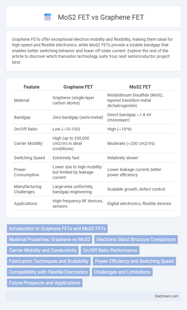
| Feature | Graphene FET | MoS2 FET |
|---|---|---|
| Material | Graphene (single-layer carbon atoms) | Molybdenum Disulfide (MoS2, layered transition metal dichalcogenide) |
| Bandgap | Zero bandgap (semi-metal) | Direct bandgap ~1.8 eV (monolayer) |
| On/Off Ratio | Low (~10-100) | High (~10^6) |
| Carrier Mobility | High (up to 200,000 cm2/Vs in ideal conditions) | Moderate (~200 cm2/Vs) |
| Switching Speed | Extremely fast | Relatively slower |
| Power Consumption | Lower due to high mobility but limited by leakage current | Lower leakage current, better power efficiency |
| Manufacturing Challenges | Large-area uniformity, bandgap engineering | Scalable growth, defect control |
| Applications | High-frequency RF devices, sensors | Digital electronics, flexible devices |
Introduction to Graphene FETs and MoS2 FETs
Graphene FETs utilize graphene's exceptional electrical conductivity and high carrier mobility, enabling fast switching speeds and enhanced device performance in nanoscale transistors. MoS2 FETs leverage the intrinsic bandgap of molybdenum disulfide, providing better current saturation and lower off-state leakage compared to graphene, which is crucial for digital logic applications. Both materials offer unique advantages for next-generation field-effect transistors, with graphene excelling in high-frequency analog circuits and MoS2 suited for low-power electronics.
Material Properties: Graphene vs MoS2
Graphene exhibits exceptional electrical conductivity and high carrier mobility due to its zero bandgap structure, making it ideal for high-speed electronic applications. In contrast, MoS2 features a sizable direct bandgap (~1.8 eV in monolayer form), enabling superior switching capabilities and low off-state current in field-effect transistors (FETs). Your choice between Graphene FET and MoS2 FET depends on balancing the need for high conductivity versus efficient switching and low power consumption.
Electronic Band Structure Comparison
Graphene FETs exhibit a zero bandgap with a linear energy-momentum dispersion, resulting in high carrier mobility but limited transistor on/off ratio. MoS2 FETs possess a direct bandgap of approximately 1.8 eV in monolayer form, enabling efficient switching behavior and strong current modulation. The intrinsic semiconducting nature of MoS2 offers superior device performance in digital applications compared to the semi-metallic, gapless graphene.
Carrier Mobility and Conductivity
Graphene FETs exhibit exceptionally high carrier mobility, often exceeding 10,000 cm2/V*s, due to the material's zero-bandgap and linear energy dispersion, enabling rapid electron transport and high conductivity. In contrast, MoS2 FETs typically have lower carrier mobility, around 200 cm2/V*s, but benefit from a sizable bandgap (~1.8 eV), which enhances current modulation and reduces leakage currents despite its relatively lower conductivity. The trade-off between graphene's superior mobility and MoS2's semiconducting properties defines their respective advantages for high-speed and low-power electronic applications.
On/Off Ratio Performance
Graphene FETs exhibit high electron mobility but suffer from a low On/Off ratio due to the absence of an inherent bandgap, limiting their effectiveness in digital switching applications. MoS2 FETs, with an intrinsic bandgap of approximately 1.8 eV in monolayer form, offer significantly higher On/Off ratios, often exceeding 10^6, making them suitable for low-power and high-performance electronics. Your choice between these devices depends on prioritizing speed and conductivity versus switching efficiency and energy consumption.
Fabrication Techniques and Scalability
Graphene FETs utilize chemical vapor deposition (CVD) and mechanical exfoliation for fabrication, providing atomically thin channels but facing challenges in uniform large-area production. MoS2 FETs benefit from scalable methods such as liquid-phase exfoliation and metal-organic chemical vapor deposition (MOCVD), enabling more consistent wafer-scale device integration. Your choice depends on the balance between graphene's superior electrical mobility and MoS2's compatibility with scalable semiconductor manufacturing.
Power Efficiency and Switching Speed
Graphene FETs exhibit superior switching speeds due to their exceptional carrier mobility exceeding 200,000 cm2/V*s, enabling rapid electron transport compared to MoS2 FETs, which have lower mobility around 200 cm2/V*s. However, MoS2 FETs offer enhanced power efficiency with steep subthreshold slopes near 60 mV/decade and lower leakage currents, making them suitable for low-power applications. The intrinsic bandgap of MoS2 enables better off-state control, while graphene's zero bandgap limits its power efficiency despite faster switching capabilities.
Compatibility with Flexible Electronics
Graphene FETs exhibit exceptional mechanical flexibility and high carrier mobility, making them highly compatible with flexible electronics for wearable and foldable devices. MoS2 FETs offer easier integration with existing semiconductor processes due to their inherent semiconducting bandgap, enhancing performance stability on flexible substrates. Both materials enable advanced flexible electronic applications, but MoS2 FETs provide superior on/off current ratios, which are crucial for low-power flexible circuits.
Challenges and Limitations
Graphene FETs face challenges such as the absence of an intrinsic bandgap, which results in poor ON/OFF current ratios and limits digital switch performance. MoS2 FETs overcome this with a sizable bandgap, but suffer from lower carrier mobility and contact resistance issues that affect device speed and power efficiency. Both materials encounter difficulties in large-scale production, uniformity control, and integration with existing silicon technology for commercial applications.
Future Prospects and Applications
Graphene FETs offer exceptional electron mobility and flexibility, making them ideal for future high-speed electronics and flexible wearable devices, while MoS2 FETs provide superior semiconductor bandgaps for low-power and high-performance digital applications. Your choice depends on balancing graphene's conductivity advantages with MoS2's energy efficiency in nanoscale transistors and sensors. Emerging applications include ultra-fast communication systems, flexible displays for graphene, and energy-efficient logic devices for MoS2 technology.
Graphene FET vs MoS2 FET Infographic