Band-edge emission results from electron-hole recombination near the semiconductor's conduction and valence bands, producing sharp, high-energy light typically close to the material's bandgap. Deep-level emission involves defects or impurities within the bandgap causing lower-energy, broader spectral features; discover how these differences impact your optoelectronic device performance in the article ahead.
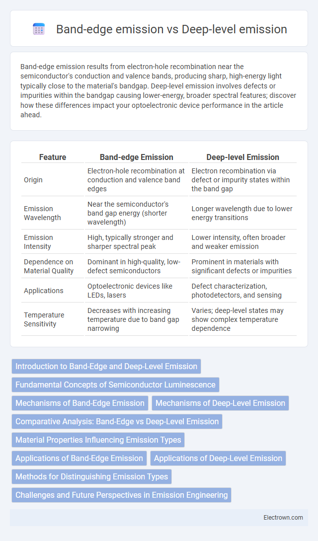
Table of Comparison
| Feature | Band-edge Emission | Deep-level Emission |
|---|---|---|
| Origin | Electron-hole recombination at conduction and valence band edges | Electron recombination via defect or impurity states within the band gap |
| Emission Wavelength | Near the semiconductor's band gap energy (shorter wavelength) | Longer wavelength due to lower energy transitions |
| Emission Intensity | High, typically stronger and sharper spectral peak | Lower intensity, often broader and weaker emission |
| Dependence on Material Quality | Dominant in high-quality, low-defect semiconductors | Prominent in materials with significant defects or impurities |
| Applications | Optoelectronic devices like LEDs, lasers | Defect characterization, photodetectors, and sensing |
| Temperature Sensitivity | Decreases with increasing temperature due to band gap narrowing | Varies; deep-level states may show complex temperature dependence |
Introduction to Band-Edge and Deep-Level Emission
Band-edge emission occurs when electrons recombine with holes near the conduction and valence band edges, producing photons with energy close to the semiconductor bandgap. Deep-level emission arises from radiative recombination involving defect states or impurities located within the bandgap, resulting in lower-energy photons. Understanding the distinction between band-edge and deep-level emissions is critical for optimizing optoelectronic device performance and identifying material quality in semiconductor physics.
Fundamental Concepts of Semiconductor Luminescence
Band-edge emission in semiconductor luminescence occurs when electrons recombine with holes directly across the bandgap, resulting in photon emission with energy close to the material's bandgap energy. Deep-level emission, on the other hand, arises from electron-hole recombination involving defect states or impurities within the bandgap, producing lower-energy photons and broader emission spectra. Understanding these emission mechanisms is crucial for tailoring optoelectronic device performance, such as LEDs and laser diodes, by controlling defect densities and band structure properties.
Mechanisms of Band-Edge Emission
Band-edge emission occurs when electrons recombine with holes directly at the edge of the conduction and valence bands, resulting in photon emission with energy close to the material's bandgap. This mechanism is highly efficient and produces sharp, well-defined luminescence spectra ideal for optoelectronic devices like LEDs and laser diodes. You can enhance band-edge emission by optimizing material purity and crystal quality to minimize non-radiative recombination pathways.
Mechanisms of Deep-Level Emission
Deep-level emission arises from electron transitions between defect states within the bandgap, which act as recombination centers capturing carriers that would otherwise contribute to band-edge emission. These defect states originate from impurities, vacancies, or interstitial atoms, introducing energy levels significantly below the conduction band or above the valence band. Non-radiative recombination often competes with radiative deep-level emission, affecting the intensity and spectral position of the emitted light.
Comparative Analysis: Band-Edge vs Deep-Level Emission
Band-edge emission originates from the recombination of electrons and holes near the semiconductor's conduction and valence band edges, producing sharp, high-energy photons with minimal energy loss. Deep-level emission arises from defects or impurities within the bandgap, resulting in broader, lower-energy photons due to trapped carriers recombining at these localized states. Your choice between band-edge and deep-level emission mechanisms significantly impacts the efficiency and wavelength stability of optoelectronic devices.
Material Properties Influencing Emission Types
Material properties such as bandgap energy, defect density, and impurity composition critically influence band-edge emission and deep-level emission in semiconductors. Band-edge emission arises from direct recombination near the conduction and valence band edges, typically favored in high-purity, defect-free materials with well-defined bandgaps. Deep-level emission, however, occurs due to radiative recombination involving defect states or impurities within the bandgap, making it prominent in materials with high defect concentrations or intentional doping; understanding these properties helps you tailor optoelectronic device performance.
Applications of Band-Edge Emission
Band-edge emission, characterized by the recombination of electrons and holes near the semiconductor's bandgap, is widely utilized in optoelectronic devices such as light-emitting diodes (LEDs) and laser diodes due to its high efficiency and specific wavelength output. This emission mechanism is critical in applications requiring narrow spectral lines and fast response times, including optical communication and high-resolution displays. Band-edge emission also plays a vital role in photovoltaic devices by enhancing charge carrier collection and improving overall solar cell performance.
Applications of Deep-Level Emission
Deep-level emission originates from defect states within the bandgap of semiconductors, making it crucial for applications in optoelectronic devices such as light-emitting diodes (LEDs) and photodetectors that require wavelength tunability. This type of emission is also exploited in radiation detectors and solar cells for enhancing sensitivity and charge carrier recombination control. Understanding and controlling deep-level emission enables your development of materials with tailored optical properties for specialized technological applications.
Methods for Distinguishing Emission Types
Photoluminescence spectroscopy is a key method for distinguishing band-edge emission from deep-level emission by analyzing the emission peak positions and intensities, with band-edge emission typically observed near the semiconductor's bandgap energy while deep-level emission occurs at lower energies due to defects. Time-resolved photoluminescence provides decay lifetimes, where band-edge emission usually shows shorter lifetimes compared to the longer, defect-related deep-level emission. Temperature-dependent measurements further aid differentiation as band-edge emissions shift predictably with temperature changes whereas deep-level emissions may show complex behavior or quenching effects.
Challenges and Future Perspectives in Emission Engineering
Band-edge emission offers high efficiency and spectral purity but struggles with stability challenges under varying environmental conditions. Deep-level emission provides tunable wavelengths and defect-related functionalities yet often suffers from non-radiative recombination losses that reduce device performance. Your future research in emission engineering should focus on developing advanced material passivation techniques and defect control strategies to enhance emission stability and efficiency for next-generation optoelectronic devices.
Band-edge emission vs Deep-level emission Infographic