Planar photodiodes provide a compact, low-capacitance design ideal for high-speed applications, while mesa photodiodes offer higher sensitivity due to their larger active area but with increased capacitance and surface leakage. Explore this article to understand how choosing between planar and mesa photodiodes can impact Your device's performance and reliability.
Table of Comparison
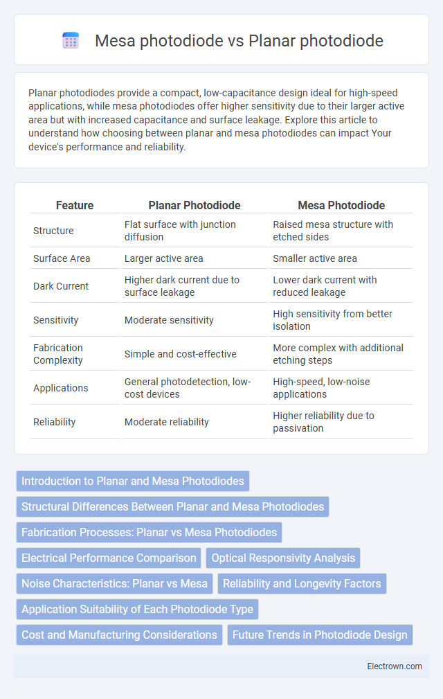
| Feature | Planar Photodiode | Mesa Photodiode |
|---|---|---|
| Structure | Flat surface with junction diffusion | Raised mesa structure with etched sides |
| Surface Area | Larger active area | Smaller active area |
| Dark Current | Higher dark current due to surface leakage | Lower dark current with reduced leakage |
| Sensitivity | Moderate sensitivity | High sensitivity from better isolation |
| Fabrication Complexity | Simple and cost-effective | More complex with additional etching steps |
| Applications | General photodetection, low-cost devices | High-speed, low-noise applications |
| Reliability | Moderate reliability | Higher reliability due to passivation |
Introduction to Planar and Mesa Photodiodes
Planar photodiodes feature a flat surface with a junction formed parallel to the wafer surface, enabling lower capacitance and faster response ideal for high-speed applications. Mesa photodiodes have a raised or etched structure, increasing surface area and junction depth, which enhances sensitivity but may cause higher dark current and noise. Your choice depends on balancing speed and sensitivity requirements for optoelectronic devices.
Structural Differences Between Planar and Mesa Photodiodes
Planar photodiodes feature a flat surface with the active junction formed beneath the semiconductor surface, providing enhanced protection and reliability against environmental damage. Mesa photodiodes have an etched, raised mesa structure that exposes the junction edges, allowing for efficient current collection but increasing susceptibility to surface defects and leakage currents. Your choice depends on application needs, where planar designs offer better stability and mesa designs provide potentially higher sensitivity.
Fabrication Processes: Planar vs Mesa Photodiodes
Planar photodiodes feature a fabrication process where the p-n junction is created by diffusing dopants into the silicon surface, resulting in a flat device structure with minimized surface recombination and improved reliability. Mesa photodiodes involve etching around the active area to form a raised mesa structure, which exposes the junction edges and increases surface recombination, potentially affecting performance. The planar approach typically offers simpler passivation and more robust devices, while mesa fabrication provides easier isolation but requires careful edge treatment to reduce leakage currents.
Electrical Performance Comparison
Planar photodiodes typically offer lower dark current and better noise performance compared to Mesa photodiodes due to their reduced surface area and minimized surface recombination. Mesa photodiodes often exhibit higher capacitance and leakage current, which can degrade signal-to-noise ratio, especially in low-light conditions. Optimizing your application's electrical performance often involves choosing planar photodiodes for improved sensitivity and stability.
Optical Responsivity Analysis
Planar photodiodes exhibit higher optical responsivity due to their reduced surface recombination and larger active area exposed to incident light compared to mesa photodiodes. Mesa photodiodes often suffer from increased surface states and recombination losses at the etched sidewalls, which degrade their responsivity performance. Optimizing the planar structure enhances carrier collection efficiency, making it more suitable for applications requiring superior optical sensitivity.
Noise Characteristics: Planar vs Mesa
Planar photodiodes generally exhibit lower noise levels compared to mesa photodiodes due to their reduced surface leakage currents and minimized edge defects. Mesa photodiodes often have increased surface recombination and leakage paths, which contribute to higher dark current noise and degraded signal-to-noise ratios. Understanding these noise characteristics helps optimize your photodetector choice for applications requiring high sensitivity and low noise performance.
Reliability and Longevity Factors
Planar photodiodes exhibit higher reliability and longer operational lifespan compared to mesa photodiodes due to their reduced surface damage and minimized leakage currents. The planar structure's passivated surfaces effectively protect against environmental contaminants and electrical stress, enhancing device stability over time. Mesa photodiodes, with exposed sidewalls, are more susceptible to surface recombination and degradation, leading to decreased longevity and increased failure rates under prolonged use.
Application Suitability of Each Photodiode Type
Planar photodiodes excel in high-speed optical communication due to their low junction capacitance and surface passivation, making them ideal for fiber-optic receivers and laser rangefinders. Mesa photodiodes offer superior sensitivity and higher breakdown voltage, which suits high-power photodetection applications like industrial sensors and avalanche photodiode arrays. The choice between planar and mesa types depends on trade-offs in response speed, sensitivity, and operational voltage requirements specific to the application.
Cost and Manufacturing Considerations
Planar photodiodes generally have lower manufacturing costs due to simpler fabrication processes and fewer etching steps compared to mesa photodiodes, which require precise, deeper etching and isolation techniques. Mesa photodiodes often exhibit better performance characteristics, but their complex structure increases production time and expenses. Choosing between planar and mesa photodiodes depends on balancing cost constraints with performance requirements in semiconductor manufacturing.
Future Trends in Photodiode Design
Emerging trends in photodiode design emphasize enhancing sensitivity and reducing noise, with planar photodiodes favored for their lower dark current due to minimized surface recombination, while mesa photodiodes continue to evolve with advanced passivation techniques to improve performance in high-speed applications. Integration of novel materials such as graphene and perovskites is expected to push the boundaries of spectral responsiveness and quantum efficiency, particularly within planar architectures due to their compatibility with existing semiconductor processes. Future photodiode innovation centers on optimizing device structure for better thermal management and scalability in photonic integrated circuits, leveraging planar designs for cost-effective mass production and mesa designs for niche, high-performance sensors.
Planar photodiode vs Mesa photodiode Infographic