Epi-ready wafers feature a highly polished surface and an optimized substrate designed for epitaxial layer deposition, ensuring superior crystal quality and device performance, while bare wafers lack this surface preparation and are typically used as substrates or for other manufacturing steps. Discover how choosing between epi-ready and bare wafers can impact your semiconductor fabrication process by reading the rest of this article.
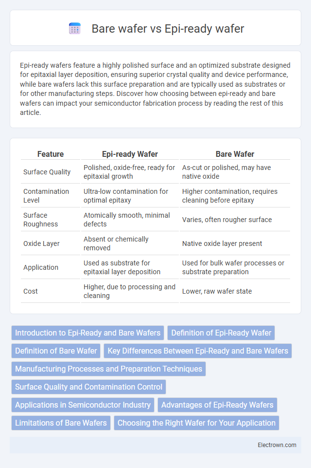
Table of Comparison
| Feature | Epi-ready Wafer | Bare Wafer |
|---|---|---|
| Surface Quality | Polished, oxide-free, ready for epitaxial growth | As-cut or polished, may have native oxide |
| Contamination Level | Ultra-low contamination for optimal epitaxy | Higher contamination, requires cleaning before epitaxy |
| Surface Roughness | Atomically smooth, minimal defects | Varies, often rougher surface |
| Oxide Layer | Absent or chemically removed | Native oxide layer present |
| Application | Used as substrate for epitaxial layer deposition | Used for bulk wafer processes or substrate preparation |
| Cost | Higher, due to processing and cleaning | Lower, raw wafer state |
Introduction to Epi-Ready and Bare Wafers
Epi-ready wafers are silicon substrates specifically prepared with an ultra-clean, defect-free surface ideal for epitaxial layer growth, ensuring high-quality semiconductor devices. Bare wafers, by contrast, refer to untreated silicon wafers lacking the specialized surface conditioning required for epitaxy, often used in general semiconductor manufacturing. Understanding the distinction between epi-ready and bare wafers is crucial for optimizing Your fabrication process and achieving superior electronic performance.
Definition of Epi-Ready Wafer
Epi-ready wafer refers to a semiconductor substrate that has undergone specialized surface treatments and cleaning processes to ensure an ultra-flat, defect-free surface ideal for epitaxial layer growth. Unlike a bare wafer, which is a raw semiconductor substrate without such preparation, an epi-ready wafer's surface is optimized for the uniform deposition of epitaxial layers critical in high-performance device fabrication. Your choice of an epi-ready wafer ensures improved crystal quality and device reliability in semiconductor manufacturing applications.
Definition of Bare Wafer
A bare wafer is a thin slice of semiconductor material, such as silicon, that serves as the substrate for integrated circuits without any epitaxial layers grown on its surface. It is typically polished and cleaned, providing a smooth and uniform base for subsequent fabrication steps in semiconductor device manufacturing. Bare wafers differ from epi-ready wafers, which have been specifically prepared to support high-quality epitaxial layer growth.
Key Differences Between Epi-Ready and Bare Wafers
Epi-ready wafers feature a polished, defect-free surface specially prepared for epitaxial layer growth, ensuring improved crystal quality and device performance compared to bare wafers, which have a standard polished surface not optimized for epitaxy. The surface contamination and native oxide levels on epi-ready wafers are meticulously controlled, whereas bare wafers may require additional cleaning steps before epitaxial processing. Your semiconductor manufacturing process benefits from higher uniformity and reduced defect density when using epi-ready wafers versus bare wafers.
Manufacturing Processes and Preparation Techniques
Epi-ready wafers undergo a specialized manufacturing process that includes high-purity surface preparation and oxide stripping to ensure an ideal substrate for epitaxial growth, whereas bare wafers are standard silicon substrates without these advanced surface treatments. The preparation technique for epi-ready wafers involves rigorous cleaning and surface conditioning to achieve atomic-level smoothness, optimizing uniform deposition of the epitaxial layer. Your choice between epi-ready and bare wafers directly impacts the quality and performance of subsequent semiconductor device fabrication, especially in applications requiring defect-free epitaxial layers.
Surface Quality and Contamination Control
Epi-ready wafers exhibit superior surface quality due to their ultra-clean, oxide-free surfaces specifically prepared for epitaxial layer growth, ensuring minimal defects and enhanced uniformity. In contrast, bare wafers may have native oxide layers or residues that increase contamination risks and hinder epitaxial deposition quality. Contamination control in epi-ready wafers involves stringent cleaning protocols and environmental controls to maintain atomic-level surface purity essential for high-performance semiconductor device fabrication.
Applications in Semiconductor Industry
Epi-ready wafers provide a pristine surface ideal for the deposition of epitaxial layers, enhancing device performance in advanced semiconductor applications such as high-speed transistors and integrated circuits. Bare wafers serve as the fundamental substrate for various semiconductor manufacturing processes but often require additional surface preparation to meet the stringent requirements of epitaxial growth. The choice between epi-ready and bare wafers significantly impacts the yield and reliability of devices in fields like power electronics, RF components, and microelectromechanical systems (MEMS).
Advantages of Epi-Ready Wafers
Epi-ready wafers offer superior surface cleanliness and atomic-level flatness compared to bare wafers, enabling enhanced epitaxial layer uniformity and reduced defect density. Their optimized surface chemistry promotes improved nucleation and growth processes, which directly improve device performance and yield. Choosing epi-ready wafers ensures your semiconductor manufacturing benefits from higher quality epitaxial layers with increased reliability and efficiency.
Limitations of Bare Wafers
Bare wafers suffer from contamination risks and surface damage during handling and processing, which can degrade device performance. Unlike epi-ready wafers that feature a pristine, defect-free surface ideal for epitaxial layer growth, bare wafers lack this preparation, limiting their suitability for advanced semiconductor manufacturing. Your production yield and device reliability may be compromised if using bare wafers for epitaxial processes due to these inherent limitations.
Choosing the Right Wafer for Your Application
Epi-ready wafers offer a pristine surface with an epitaxial-ready silicon layer, essential for applications requiring high-quality epitaxial film growth and superior device performance. Bare wafers, lacking this epitaxial surface, are ideal for processes that involve oxidation, diffusion, or polycrystalline layer deposition, making them cost-effective for less demanding applications. Selecting between epi-ready and bare wafers depends on the specific requirements of device fabrication, such as electrical characteristics, layer uniformity, and overall process compatibility.
Epi-ready wafer vs Bare wafer Infographic