II-VI semiconductors, composed of elements from groups II and VI, are known for their tunable band gaps and strong optical properties, making them ideal for devices like LEDs and photodetectors. III-V semiconductors, combining elements from groups III and V, offer high electron mobility and direct band gaps, which are crucial for high-speed electronics and optoelectronics; discover more about how both materials impact your technology choices in the full article.
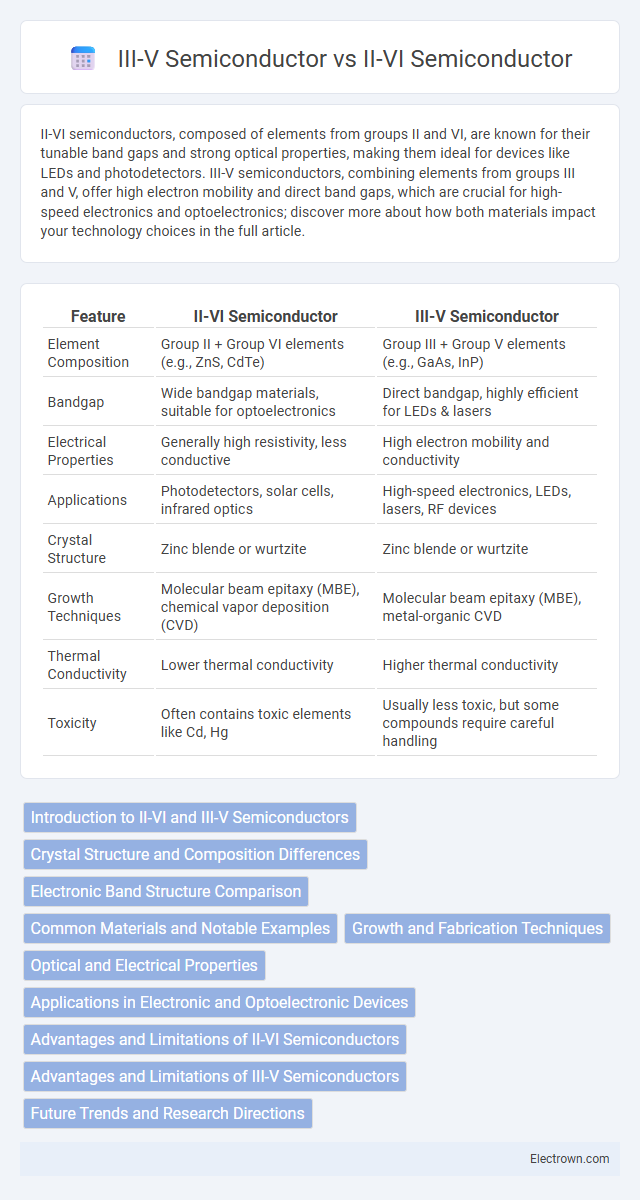
Table of Comparison
| Feature | II-VI Semiconductor | III-V Semiconductor |
|---|---|---|
| Element Composition | Group II + Group VI elements (e.g., ZnS, CdTe) | Group III + Group V elements (e.g., GaAs, InP) |
| Bandgap | Wide bandgap materials, suitable for optoelectronics | Direct bandgap, highly efficient for LEDs & lasers |
| Electrical Properties | Generally high resistivity, less conductive | High electron mobility and conductivity |
| Applications | Photodetectors, solar cells, infrared optics | High-speed electronics, LEDs, lasers, RF devices |
| Crystal Structure | Zinc blende or wurtzite | Zinc blende or wurtzite |
| Growth Techniques | Molecular beam epitaxy (MBE), chemical vapor deposition (CVD) | Molecular beam epitaxy (MBE), metal-organic CVD |
| Thermal Conductivity | Lower thermal conductivity | Higher thermal conductivity |
| Toxicity | Often contains toxic elements like Cd, Hg | Usually less toxic, but some compounds require careful handling |
Introduction to II-VI and III-V Semiconductors
II-VI semiconductors, composed of elements from groups II and VI such as zinc sulfide and cadmium telluride, are known for their direct band gaps and applications in optoelectronic devices like LEDs and laser diodes. III-V semiconductors, formed from group III and V elements like gallium arsenide and indium phosphide, offer high electron mobility and are widely used in high-frequency and high-efficiency electronic components. Your choice between II-VI and III-V materials will depend on factors like desired band gap, device performance, and application-specific requirements.
Crystal Structure and Composition Differences
II-VI semiconductors typically crystallize in the zinc blende or wurtzite structures, composed of elements from group II (such as zinc or cadmium) and group VI (such as sulfur, selenium, or tellurium). III-V semiconductors form similarly stable zinc blende or wurtzite crystal lattices but consist of group III elements (like gallium or indium) combined with group V elements (such as arsenic or phosphorus). The compositional difference influences lattice constants and bandgap energies, affecting electronic and optical properties crucial for device applications.
Electronic Band Structure Comparison
II-VI semiconductors, such as ZnSe and CdTe, typically exhibit wider bandgaps ranging from 1.2 to 3.5 eV, making them suitable for optoelectronic applications in the visible to ultraviolet spectrum. III-V semiconductors like GaAs and InP generally possess direct bandgaps with values between 0.3 and 2.3 eV, enabling efficient electron mobility and high-speed electronic device performance. The distinct band alignment and effective mass differences in II-VI and III-V materials directly impact their electronic and optical properties, influencing their respective device integration and functionality.
Common Materials and Notable Examples
II-VI semiconductors commonly include materials like cadmium telluride (CdTe) and zinc selenide (ZnSe), known for their applications in optoelectronics and photovoltaics. III-V semiconductors primarily feature compounds such as gallium arsenide (GaAs) and indium phosphide (InP), widely recognized for high-speed electronics and laser technology. Your choice between II-VI and III-V materials depends on device requirements, including bandgap properties and electron mobility.
Growth and Fabrication Techniques
II-VI semiconductors primarily utilize molecular beam epitaxy (MBE) and metal-organic chemical vapor deposition (MOCVD) for precise layer-by-layer growth, enabling high-quality crystalline films essential for optoelectronic devices. III-V semiconductors also rely on MBE and MOCVD, but their fabrication often achieves higher electron mobility and integration with silicon substrates, making them pivotal in high-speed electronics and photonics. Your choice between II-VI and III-V materials should consider the compatibility of growth techniques with target device performance and integration requirements.
Optical and Electrical Properties
II-VI semiconductors, such as ZnSe and CdTe, exhibit strong direct bandgaps and high exciton binding energies, making them excellent for blue and green optoelectronic devices with superior optical emission efficiency. III-V semiconductors like GaAs and InP possess higher electron mobility and superior electrical conductivity, enabling faster electronic and optoelectronic device performance. The larger bandgap tunability in II-VI compounds supports diverse optical applications, while III-V materials dominate high-speed electronics due to their exceptional charge carrier transport properties.
Applications in Electronic and Optoelectronic Devices
II-VI semiconductors, such as ZnSe and CdTe, are extensively used in optoelectronic devices like infrared detectors, laser diodes, and photovoltaic cells due to their wide bandgaps and high photon absorption efficiency. III-V semiconductors, including GaAs and InP, dominate high-speed electronics and optoelectronics with applications in microwave transistors, light-emitting diodes (LEDs), and high-efficiency solar cells because of their superior electron mobility and direct bandgap properties. Both material classes are critical in the development of advanced electronic and optoelectronic devices, with II-VI materials excelling in wide-spectrum optical applications and III-V materials leading in high-frequency and high-efficiency light emission technologies.
Advantages and Limitations of II-VI Semiconductors
II-VI semiconductors, composed of elements such as zinc, cadmium, and sulfur, offer advantages including a wide bandgap, high electron mobility, and excellent optical properties, making them ideal for photodetectors, lasers, and solar cells. Their ability to operate at higher temperatures and provide efficient ultraviolet light emission surpasses many III-V semiconductors, which typically include elements like gallium and arsenic. However, II-VI materials often face challenges in crystal growth quality and stability, which can limit device performance and commercialization potential compared to the more mature III-V semiconductor technology.
Advantages and Limitations of III-V Semiconductors
III-V semiconductors, such as gallium arsenide (GaAs) and indium phosphide (InP), offer superior electron mobility and direct bandgaps, enabling high-speed electronic and optoelectronic devices like lasers and high-frequency transistors. These materials excel in infrared optoelectronics, high-efficiency solar cells, and high-power amplifiers, but their manufacturing costs and fragility are higher compared to silicon-based or II-VI semiconductors. Limitations include challenges in large-scale integration, lattice mismatch issues in heterostructures, and sensitivity to defects, which can impact device reliability and yield.
Future Trends and Research Directions
II-VI semiconductors are gaining traction in optoelectronics and photovoltaic applications due to their superior performance in ultraviolet and infrared wavelength ranges, with research focusing on enhancing defect control and scalability. III-V semiconductors continue to dominate high-speed electronics and optoelectronic devices, driven by innovations in quantum dot integration and nanowire technology that improve efficiency and thermal management. Your choice between II-VI and III-V materials will depend on the specific performance requirements of future applications such as 5G communications, photonic circuits, and next-generation solar cells.
II-VI semiconductor vs III-V semiconductor Infographic