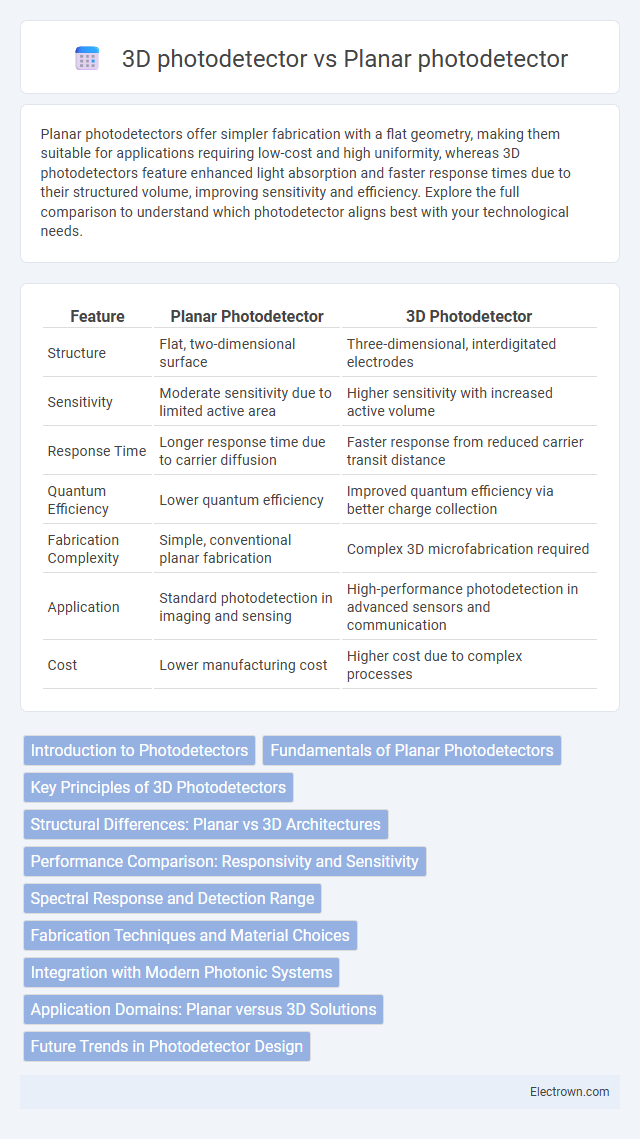
Planar photodetectors offer simpler fabrication with a flat geometry, making them suitable for applications requiring low-cost and high uniformity, whereas 3D photodetectors feature enhanced light absorption and faster response times due to their structured volume, improving sensitivity and efficiency. Explore the full comparison to understand which photodetector aligns best with your technological needs.
Table of Comparison
| Feature | Planar Photodetector | 3D Photodetector |
|---|---|---|
| Structure | Flat, two-dimensional surface | Three-dimensional, interdigitated electrodes |
| Sensitivity | Moderate sensitivity due to limited active area | Higher sensitivity with increased active volume |
| Response Time | Longer response time due to carrier diffusion | Faster response from reduced carrier transit distance |
| Quantum Efficiency | Lower quantum efficiency | Improved quantum efficiency via better charge collection |
| Fabrication Complexity | Simple, conventional planar fabrication | Complex 3D microfabrication required |
| Application | Standard photodetection in imaging and sensing | High-performance photodetection in advanced sensors and communication |
| Cost | Lower manufacturing cost | Higher cost due to complex processes |
Introduction to Photodetectors
Planar photodetectors feature a flat junction design that provides efficient light absorption and fast response times, making them suitable for traditional optoelectronic applications. In contrast, 3D photodetectors employ vertically structured architectures that increase the active surface area, enhancing light capture and sensitivity for advanced imaging and sensing technologies. Your choice between planar and 3D photodetectors depends on the required performance attributes such as speed, sensitivity, and device integration complexity.
Fundamentals of Planar Photodetectors
Planar photodetectors operate on the principle of light absorption within a two-dimensional semiconductor layer, where photogenerated carriers are collected across a lateral junction. Their fabrication involves standard lithography techniques, enabling precise control over layer thickness and doping profiles to optimize responsivity and speed. The planar structure typically results in lower dark current and simpler integration with existing IC technology compared to 3D photodetectors.
Key Principles of 3D Photodetectors
3D photodetectors enhance light absorption by incorporating vertical nanostructures that increase the active surface area compared to planar photodetectors, which rely on flat, two-dimensional surfaces. The vertical architecture of 3D photodetectors facilitates shorter carrier collection paths, improving charge carrier mobility and reducing recombination losses. This design results in higher responsivity, faster response times, and better performance under low-light conditions relative to traditional planar photodetectors.
Structural Differences: Planar vs 3D Architectures
Planar photodetectors feature a flat, layered structure where light absorption and carrier collection occur across a uniform surface, leading to simpler fabrication but limited active area. In contrast, 3D photodetectors utilize vertically structured architectures with nanowires or pillars, significantly increasing surface area and enhancing light absorption and carrier collection efficiency. Your choice between planar and 3D designs impacts device performance, with 3D architectures offering improved sensitivity and response speed due to their optimized geometry.
Performance Comparison: Responsivity and Sensitivity
Planar photodetectors typically exhibit lower responsivity and sensitivity due to limited light absorption and carrier collection efficiency confined to a two-dimensional surface. In contrast, 3D photodetectors enhance responsivity by maximizing the active volume and enabling multiple light absorption pathways, significantly increasing sensitivity. The three-dimensional architecture reduces carrier recombination and facilitates faster charge transport, resulting in superior photodetection performance.
Spectral Response and Detection Range
Planar photodetectors typically offer a narrower spectral response and limited detection range due to their surface-level charge collection, making them less efficient in absorbing longer wavelengths. In contrast, 3D photodetectors, with their vertically structured electrodes, enhance light absorption and carrier collection across a broader spectral range, especially in the infrared region. This architecture significantly extends the detection range and improves sensitivity compared to traditional planar designs.
Fabrication Techniques and Material Choices
Planar photodetectors utilize traditional fabrication techniques such as lithography and thin-film deposition on flat substrates, often employing materials like silicon, GaAs, or perovskites for efficient charge transport and light absorption. In contrast, 3D photodetectors leverage advanced fabrication methods including 3D printing, nanowire growth, or templated self-assembly, incorporating materials such as semiconducting nanowires, quantum dots, or hybrid organic-inorganic compounds to enhance surface area and improve photoresponsivity. Material choices in 3D photodetectors focus on complex morphologies to optimize light trapping and carrier collection, whereas planar devices prioritize uniformity and scalability in semiconductor films.
Integration with Modern Photonic Systems
Planar photodetectors offer straightforward integration with traditional planar photonic circuits, leveraging mature fabrication processes for cost-effective mass production. In contrast, 3D photodetectors enable enhanced light absorption and improved responsivity by utilizing vertical architectures, which can be seamlessly integrated into complex modern photonic systems requiring compact, high-performance components. The choice between planar and 3D photodetectors depends on system requirements for sensitivity, footprint, and compatibility with existing photonic integration platforms.
Application Domains: Planar versus 3D Solutions
Planar photodetectors are widely utilized in applications requiring high-resolution imaging and optical communication due to their mature fabrication processes and planar geometry compatible with CMOS technology. 3D photodetectors excel in domains demanding enhanced light absorption and sensitivity, such as LiDAR, biomedical imaging, and low-light sensing, by exploiting their vertical architecture to increase quantum efficiency. The choice between planar and 3D photodetector solutions depends on specific application requirements like sensitivity, integration complexity, and device footprint.
Future Trends in Photodetector Design
Future trends in photodetector design emphasize 3D photodetectors due to their superior light absorption and enhanced carrier collection efficiency compared to planar photodetectors. Innovations in nanostructuring and advanced materials like perovskites enable 3D architectures to achieve higher sensitivity, faster response times, and better integration with optoelectronic systems. Research continues to focus on optimizing these 3D designs for flexible, wearable, and high-resolution imaging applications, outperforming traditional planar devices in scalability and performance.
Planar photodetector vs 3D photodetector Infographic